SCAN926260TUF/NOPB National Semiconductor, SCAN926260TUF/NOPB Datasheet
SCAN926260TUF/NOPB
Specifications of SCAN926260TUF/NOPB
*SCAN926260TUF/NOPB
SCAN926260TUF
Available stocks


Related parts for SCAN926260TUF/NOPB

SCAN926260TUF/NOPB Summary of contents
Page 1
... The SCAN926260 integrates six 10-bit deserializer devices into a single chip. The SCAN926260 can simultaneously de- serialize up to six data streams that have been serialized by National Semiconductor’s 10-bit Bus LVDS serializers. In ad- dition, the SCAN926260 is compliant with IEEE standard 1149.1 and also features an At-Speed Built-In Self Test (BIST). For more details, please see the sections titled " ...
Page 2
... Absolute Maximum Ratings If Military/Aerospace specified devices are required, please contact the National Semiconductor Sales Office/ Distributors for availability and specifications. Supply Voltage ( BLVDS Input Voltage (Rin ±) Maximum Package Power Dissipation Capacity @ 25°C Package Thermal Resistance θ 196 LBGA: JA θ ...
Page 3
Symbol Parameter Supply Current Checker Board I Total Supply Current CCR Reduction in Supply Checker Board ΔI CCR Current per Channel MS_PWRDN= Total Supply Current I CCXR when Powered Down Timing Requirements for REFCLK t REFCLK Period RFCP t REFCLK ...
Page 4
Note 1: “Absolute Maximum Ratings” are those values beyond which the safety of the device cannot be guaranteed. They are not meant to imply that the devices should be operated at these limits. The table of “Electrical Characteristics” specifies conditions ...
Page 5
Timing Diagrams FIGURE 2. Output Timing t FIGURE 3. Deserializer CMOS/LVTTL Output Load and Transition Times FIGURE 1. Deserializer Delay t DD 20028307 and t (Data Valid) ROS ROH 5 20028304 20028331 www.national.com ...
Page 6
FIGURE 4. Locktime from PWRDNn t FIGURE 5. Locktime to SYNCPAT t DSR2 FIGURE 6. Loss of Lock 6 20028309 DSR1 20028311 20028313 ...
Page 7
FIGURE 7. Deserializer TRI-STATE Test Circuit and Timing Note: For an explanation of Ideal Crossing Point and Noise Margin, please see the Application Information section. FIGURE 8. Deserializer Noise Margin and Sampling Window 20028330 7 20028318 www.national.com ...
Page 8
... Functional Description The SCAN926260 combines six 1:10 deserializers into a sin- gle chip. Each of the six deserializers accepts a Bus LVDS data stream from National Semiconductor's DS92LV1021, DS92LV1023, DS92LV8028, SCAN921023, or SCAN921025 Serializer. The deserializers then recover the clock and data to deliver the resulting 10-bit wide words to the outputs. ...
Page 9
Initialization Before the SCAN926260 receives and deserializes data, it and the transmitting Serializer must initialize the link. Initial- ization refers to synchronizing the Serializer's and the Deserializer's PLL's to local clocks. The local clocks must be within ±5% of the ...
Page 10
SCAN926260 Control Signal Truth Table SCAN Mode Internal Signals STATE SCAN_HIZB SCAN_BIST SCAN 0 (Note 1) SCAN 1 (Note 1) Powerdown 1 (Note 2) Powerdown 1 (Note 3) Normal, Not Locked 1 (Note 5) Normal, Locked 1 (Note 5) REN ...
Page 11
IEEE 1149.1 Test Modes The SCAN926260 features interconnect test access that is compliant to the IEEE 1149.1 Standard for Boundary Scan Test (JTAG). All digital TTL I/O's on the device are accessible using IEEE 1149.1, and entering this test mode ...
Page 12
Application Information USING THE SCAN926260 The SCAN926260 combines six 1:10 deserializers into a sin- gle chip. Each of the six deserializers accepts a BusLVDS data stream up to 660 Mbps from one of National Semiconductor's 10-Bit Serializers. The Deserializers then ...
Page 13
Failsafe Biasing. Please see Figure 11 for the Failsafe Biasing Setup. DIFFERENCES BETWEEN the DS92LV1260, the SCAN921260, and the SCAN926260 The DS92LV1260 is a six channel, ten bit, Bus LVDS Dese- rializer with random lock capability and a parallel ...
Page 14
CLC). If employed, a separate pie filter is recom- mended for each PLL to minimize drop in potential due to the series resistance. Separate power planes for the PVDD pins is typically not required. AVDD = LVDS SECTION ...
Page 15
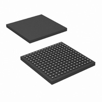
Pin Diagram Note OVERBAR Top View of SCAN926260TUF (196 pin LBGA) 15 20028314 www.national.com ...
Page 16
Pin Descriptions Pin Name Type GND GND Bus LVDS R ± INn Input N/C DVdd DGND PVdd PGND AVdd AGND 3.3V CMOS PWRDWN [0:5] Input 3.3V CMOS MS_PWRDWN Input 3.3V CMOS REN Input 3.3V CMOS REFCLK Input 3.3V CMOS LOCK[0:5] ...
Page 17
Pin Name Type 3.3V CMOS TMS Input 3.3V CMOS TRST Input 3.3V CMOS TDI Input 3.3V CMOS TCK Input 3.3V CMOS TDO Output 3.3V CMOS BISTMODE_REQ Input 3.3V CMOS BIST_SEL[0:2] Input 3.3V CMOS BIST_ACT Input N/C Pins Test Mode Select ...
Page 18
Physical Dimensions www.national.com inches (millimeters) unless otherwise noted Order Number SCAN926260TUF (Tray) Order Number SCAN926260TUFX (Tape and Reel) NS Package Number UJB196A 18 ...
Page 19
Notes 19 www.national.com ...
Page 20
... For more National Semiconductor product information and proven design tools, visit the following Web sites at: Products Amplifiers www.national.com/amplifiers Audio www.national.com/audio Clock Conditioners www.national.com/timing Data Converters www.national.com/adc Displays www.national.com/displays Ethernet www.national.com/ethernet Interface www.national.com/interface LVDS www.national.com/lvds Power Management www.national.com/power Switching Regulators www.national.com/switchers LDOs www ...