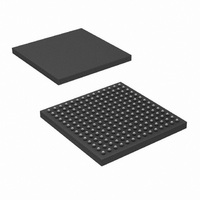
SCAN928028TUF/NOPB National Semiconductor, SCAN928028TUF/NOPB Datasheet - Page 10

SCAN928028TUF/NOPB
Manufacturer Part Number
SCAN928028TUF/NOPB
Description
IC SERIALIZER 8CH 10:1 196-LBGA
Manufacturer
National Semiconductor
Series
SCANr
Datasheet
1.SCAN928028TUFNOPB.pdf
(20 pages)
Specifications of SCAN928028TUF/NOPB
Function
Serializer
Data Rate
480Mbps
Input Type
LVDS
Output Type
LVDS
Number Of Inputs
10
Number Of Outputs
1
Voltage - Supply
3 V ~ 3.6 V
Operating Temperature
-40°C ~ 85°C
Mounting Type
Surface Mount
Package / Case
196-LBGA
Lead Free Status / RoHS Status
Lead free / RoHS Compliant
Other names
*SCAN928028TUF
*SCAN928028TUF/NOPB
SCAN928028TUF
*SCAN928028TUF/NOPB
SCAN928028TUF
Available stocks
Company
Part Number
Manufacturer
Quantity
Price
Company:
Part Number:
SCAN928028TUF/NOPB
Manufacturer:
National Semiconductor
Quantity:
135
Company:
Part Number:
SCAN928028TUF/NOPB
Manufacturer:
NSC
Quantity:
105
Company:
Part Number:
SCAN928028TUF/NOPB
Manufacturer:
Texas Instruments
Quantity:
10 000
www.national.com
The user has the choice of allowing the deserializer to resyn-
chronize to the data stream, or to force synchronization by
pulsing the Serializer SYNC pin. This scheme is left up to the
user discretion.
POWER-DOWN
The Power-down state is a low power sleep mode that the
Serializer and Deserializer typically occupy while waiting for
initialization, or to reduce power when there are no pending
data transfers. The SCAN928028 serializers enter Power-
down when MS_PWDN is driven low. In Power-down, the PLL
stops and the outputs go into TRI-STATE. To exit Power-
down, the system drives MS_PWDN high.
Each of the serializers in the '8028 also has an individual
power down, PWDNn control pin. This control enables the
deactivation of individual serializers while allowing others to
operate normally. The benefit is that spare serializers can be
allocated for backup operation, but not consuming power until
employed for data transfers.
The Individual Power Down will NOT cause the PLL of the
device to lose lock, but it will cause the specific serializer
channel to go into a low power sleep mode and its output go
into TRI-STATE. Thus, the device will NOT go through the
Initialization state when individual channels exit the Individual
Power Down state, and the output of the specific channel will
become available after a short delay, see Figure 7 and spec
t
TRI-STATE
When the system drives DEN pin low, the serializer outputs
enter TRI-STATE. This will TRI-STATE the output pins (DO0
± to DO7±). When the system drives DEN high, the serializers
will return to the previous state as long as all other control pins
remain static (PWDNn, TCLK, SYNCn, and DINn[0:9]).
TEST FEATURES
Since the high-speed LVDS serial data transmission line qual-
ity is essential to the chipset operation, a means of checking
this signal integrity is built into the SCAN928028 serializer.
Each Serializer channel has the ability to transfer an internally
generated PRBS data pattern. This pattern traverses the
ICR
10
transmission line to the deserializer. Specific deserializers
(SCAN921224 for example) have the complement PRBS pat-
tern verification circuit. The deserializer checks the data pat-
tern for bit errors and reports any errors on the test verification
pins on the deserializer.
The @SPEED feature uses 5 signal pins. The BIST_SEL[0:3]
and BIST_ACT pins together determine the functions of the
BIST mode. The BIST_ACT signal activates the test feature.
The BIST_SEL[0:3] selects 1 of 8 channels as the output for
the BIST pattern. All channels perform BIST when BIST_ACT
= H and BIST_SEL<0:3>=08H.
JTAG TEST FEATURES
In addition to using IEEE 1149.1 test access to the digital TTL
pins, the SCAN928028 has two instructions to test the LVDS
interconnects. The first instruction is EXTEST. This is imple-
mented at LVDS levels and is only intended as a go no-go
test (e.g. missing cables). The second method is the RUN-
BIST instruction. It is an "at-system-speed" interconnect test.
It is executed in approximately 33mS with a maximum system
clock speed of 66MHz. There are two bits in the RX BIST data
register for notification of PASS/FAIL and TEST_COM-
PLETE. Pass indicates that the BER (Bit-Error-Rate) is better
than 10
An important detail is that once both devices have the RUN-
BIST instruction loaded into their respective instruction reg-
isters, both devices must move into the RTI (Run-Test-Idle)
state within 4K system clocks (At a TCLK of 66Mhz and TCK
of 1MHz this allows for 66 TCK cycles). This is not a concern
when both devices are on the same scan chain or LSP, how-
ever, it can be a problem with some multi-drop devices. This
test mode has been simulated and verified using National's
SCANSTA111.
If the user is unable to meet the constraint of moving both taps
into RTI within 4K system clocks, the receiver must be moved
into the RTI state first. The receiver can then stay in RTI in-
definitely until the transmitter is moved into RTI and the BIST
pattern begins. This is true for either SCAN initiated BIST or
pin initiated BIST_ALONE or any combination of the two.
-7
.


