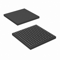
DS92LV1260TUJB/NOPB National Semiconductor, DS92LV1260TUJB/NOPB Datasheet - Page 15

DS92LV1260TUJB/NOPB
Manufacturer Part Number
DS92LV1260TUJB/NOPB
Description
IC DESRL 6CH 10BIT BLVDS 196LBGA
Manufacturer
National Semiconductor
Datasheet
1.DS92LV1260TUJBNOPB.pdf
(17 pages)
Specifications of DS92LV1260TUJB/NOPB
Function
Deserializer
Data Rate
480Mbps
Input Type
LVDS
Output Type
LVTTL
Number Of Inputs
10
Number Of Outputs
1
Voltage - Supply
3 V ~ 3.6 V
Operating Temperature
-40°C ~ 85°C
Mounting Type
Surface Mount
Package / Case
196-LBGA
Lead Free Status / RoHS Status
Lead free / RoHS Compliant
Other names
*DS92LV1260TUJB
*DS92LV1260TUJB/NOPB
DS92LV1260TUJB
*DS92LV1260TUJB/NOPB
DS92LV1260TUJB
Available stocks
Company
Part Number
Manufacturer
Quantity
Price
Company:
Part Number:
DS92LV1260TUJB/NOPB
Manufacturer:
Texas Instruments
Quantity:
10 000
B2,B14
C12,C13,B13
A4-A3, C6-C5, A7-A6,
C9-C8, A10-A9,
C11-C10, A13-A12
D12
F12
B12,A14,D10
B11
C7
B9
A11
B7
A8
B8
A5
B6
D7
B5
C4
A2
B4
D5
A1
B1
D6
B3
C3
F3,P1,N3,P12,P13,D13
E6,J5,K5,K10,J10,E9
Pin Descriptions
Pins
LOCK (0:5)
RCLK_R/F
Pin Name
SEL (0:2)
Rin(n) +/-
REFCLK
PWRDN
CHTST
DGND
DGND
DGND
PGND
AGND
AGND
AGND
AGND
AGND
PVdd
AVdd
AVdd
AVdd
AVdd
AVdd
DVdd
DVdd
DVdd
GND
REN
N/C
CMOS
CMOS
CMOS
CMOS
CMOS
CMOS
CMOS
LVDS
Type
GND
3.3V
3.3V
3.3V
3.3V
3.3V
3.3V
3.3V
Bus
O
O
I
I
I
I
I
I
15
GND pins for ESD structures
These pins control which Bus LVDS input is steered to the
CHTST output
Bus LVDS differential input pins
Supply voltage for PLL circuitry
Supply voltage for input buffer circuitry
GND pin for PLL circuitry
GND pin for input buffer circuitry
Supply voltage for LVDS REC.
Supply voltage for LVDS REC.
Supply voltage for Band Gap reference.
GND pin for AVDD.
GND pin for AVDD1.
GND pin for BGVDD.
GND pin for VDDI.
Supply voltage for input logic circuitry.
Tie to digital ground.
Controls whether the device is active or in ’sleep’ mode
Controls the relation of Rout data to RCLK edge: RCLK_R/F
= H setup and hold times are referred to the rising RCLK
edge; RCLK_R/F = L setup and hold times are referenced to
the falling RCLK edge.
Enables the Routn, RCLKn, and SYNCCLK outputs.
Frequency reference clock input.
GND pin for VDDO
GND for digital section.
Do not connect.
Supply voltage for digital section.
Supply voltage for digital section.
Allows low speed testing of the Rin inputs under control of
the SEL (0:2) pins.
Indicates the status of the PLLs for the individual
deserializers: LOCK= L indicates locked, LOCK= H indicates
unlicked.
Supply voltage for the logic circuitry.
Description
www.national.com


