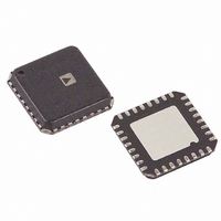
AD9943KCPZ Analog Devices Inc, AD9943KCPZ Datasheet - Page 19

AD9943KCPZ
Manufacturer Part Number
AD9943KCPZ
Description
IC CCD SIGNAL PROCESSOR 32-LFCSP
Manufacturer
Analog Devices Inc
Type
CCD Signal Processor, 10-Bitr
Datasheet
1.AD9943KCPZRL.pdf
(20 pages)
Specifications of AD9943KCPZ
Package / Case
32-LFCSP
Input Type
Logic
Output Type
Logic
Interface
3-Wire Serial
Mounting Type
Surface Mount
Supply Voltage Range
2.7V To 3.6V
Operating Temperature Range
-20°C To +85°C
Digital Ic Case Style
LFCSP
No. Of Pins
32
Svhc
No SVHC (18-Jun-2010)
Supply Voltage
RoHS Compliant
Ic Function
CCD Signal Processor
Rohs Compliant
Yes
Lead Free Status / RoHS Status
Lead free / RoHS Compliant
Current - Supply
-
Lead Free Status / RoHS Status
Lead free / RoHS Compliant
Available stocks
Company
Part Number
Manufacturer
Quantity
Price
Company:
Part Number:
AD9943KCPZ
Manufacturer:
ADI
Quantity:
585
Part Number:
AD9943KCPZ
Manufacturer:
ADI/亚德诺
Quantity:
20 000
Company:
Part Number:
AD9943KCPZRL
Manufacturer:
SANYO
Quantity:
410
Company:
Part Number:
AD9943KCPZRL
Manufacturer:
ADI
Quantity:
15 000
INTERNAL POWER-ON RESET CIRCUITRY
After power-on, the AD9943/AD9944 automatically reset all
internal registers and perform internal calibration procedures.
This takes approximately 1 ms to complete. During this time,
normal clock signals and serial write operations may occur.
However, serial register writes are ignored until the internal
reset operation is completed.
GROUNDING AND DECOUPLING
RECOMMENDATIONS
As shown in Figure 17 and Figure 18, a single ground plane is
recommended for the AD9943/AD9944. This ground plane
should be as continuous as possible. This ensures that all analog
decoupling capacitors provide the lowest possible impedance
path between the power and bypass pins and their respective
ground pins. All decoupling capacitors should be located as
OUTPUTS
DATA
12
NC = NO CONNECT
D0
D1
D2
D3
D4
D5
D6
D7
D8
D9
Figure 18. AD9944 Recommended Circuit Configuration for CCD Mode
SUPPLY
DRIVER
1
2
3
4
5
6
7
8
INTERFACE
3V
32 31 30 29 28 27 26 25
9 10
SERIAL
0.1µF
PIN 1
IDENTIFIER
11
(Not to Scale)
TOP VIEW
AD9944
12 13 14 15 16
Rev. B | Page 19 of 20
3
0.1µF
3V
ANALOG
SUPPLY
close as possible to the package pins. A single clean power
supply is recommended for the AD9943 and AD9944, but a
separate digital driver supply may be used for DRVDD (Pin 11).
DRVDD should always be decoupled to DRVSS (Pin 12), which
should be connected to the analog ground plane. Advantages of
using a separate digital driver supply include using a lower
voltage (2.7 V) to match levels with a 2.7 V ASIC, and reducing
digital power dissipation and potential noise coupling. If the
digital outputs must drive a load larger than 20 pF, buffering
is the recommended method to reduce digital code transition
noise. Alternatively, placing series resistors close to the digital
output pins may also help reduce noise.
Note: The exposed pad on the bottom of the AD9943/AD9944
should be soldered to the GND plane of the printed circuit
board.
24
23
22
21
20
19
18
17
REFB
REFT
CCDIN
AVSS
AVDD
SHD
SHP
CLPOB
0.1µF
1.0µF
1.0µF
5
CLOCK
INPUTS
0.1µF
3V
ANALOG
SUPPLY
CCDIN
AD9943/AD9944


