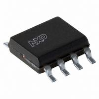
PCA9536D,118 NXP Semiconductors, PCA9536D,118 Datasheet - Page 6

PCA9536D,118
Manufacturer Part Number
PCA9536D,118
Description
IC I/O EXPANDER I2C 4B 8SOIC
Manufacturer
NXP Semiconductors
Datasheet
1.PCA9536TK118.pdf
(22 pages)
Specifications of PCA9536D,118
Package / Case
8-SOIC (3.9mm Width)
Interface
I²C, SMBus
Number Of I /o
4
Interrupt Output
No
Frequency - Clock
400kHz
Voltage - Supply
2.3 V ~ 5.5 V
Operating Temperature
-40°C ~ 85°C
Mounting Type
Surface Mount
Includes
POR
Logic Family
PCA9536
Number Of Lines (input / Output)
4.0 / 4.0
Operating Supply Voltage
2.3 V to 5.5 V
Power Dissipation
200 mW
Operating Temperature Range
- 40 C to + 85 C
Input Voltage
5 V
Logic Type
I2C, SMBus
Maximum Clock Frequency
400 KHz
Mounting Style
SMD/SMT
Number Of Input Lines
4.0
Number Of Output Lines
4.0
Output Current
50 mA
Output Voltage
5 V
Lead Free Status / RoHS Status
Lead free / RoHS Compliant
For Use With
568-3615 - DEMO BOARD I2C
Lead Free Status / Rohs Status
Lead free / RoHS Compliant
Other names
568-1835-2
935277415118
PCA9536D-T
935277415118
PCA9536D-T
NXP Semiconductors
PCA9536_5
Product data sheet
6.1.5 Register 3 - Configuration register
6.2 Power-on reset
6.3 I/O port
This register configures the directions of the I/O pins. If a bit in this register is set, the
corresponding port pin is enabled as an input with high-impedance output driver. If a bit in
this register is cleared, the corresponding port pin is enabled as an output. At reset, the
I/Os are configured as inputs with a weak pull-up to V
‘Not used’ bits can be programmed with either logic 0 or logic 1.
Table 7.
Legend: * default value
When power is applied to V
a reset condition until V
and the PCA9536 registers and state machine will initialize to their default states.
Thereafter, V
For a power reset cycle, V
operating voltage.
When an I/O is configured as an input, FETs Q1 and Q2 are off, creating a
high-impedance input with a weak pull-up (100 kΩ typical) to V
be raised above V
If the I/O is configured as an output, then either Q1 or Q2 is enabled, depending on the
state of the Output Port register. Care should be exercised if an external voltage is applied
to an I/O configured as an output because of the low-impedance paths that exist between
the pin and either V
Bit
7
6
5
4
3
2
1
0
Symbol
C7
C6
C5
C4
C3
C2
C1
C0
Register 3 - Configuration register bit description
DD
must be lowered below 0.2 V to reset the device.
DD
DD
Access
R/W
R/W
R/W
R/W
R/W
R/W
R/W
R/W
to a maximum of 5.5 V.
Rev. 05 — 25 January 2010
or V
DD
DD
has reached V
SS
DD
.
must be lowered below 0.2 V and then restored to the
, an internal Power-On Reset (POR) holds the PCA9536 in
Value
1*
1*
1*
1*
1*
1*
1*
1*
POR
Description
not used
configures the directions of the I/O pins
. At that point, the reset condition is released
0 = corresponding port pin enabled as an output
1 = corresponding port pin configured as input
(default value)
DD
4-bit I
.
2
C-bus and SMBus I/O port
DD
. The input voltage may
PCA9536
© NXP B.V. 2010. All rights reserved.
6 of 22


