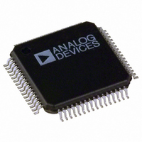
ADV7303AKST Analog Devices Inc, ADV7303AKST Datasheet - Page 34

ADV7303AKST
Manufacturer Part Number
ADV7303AKST
Description
IC DAC VIDEO HDTV 6-11BIT 64LQFP
Manufacturer
Analog Devices Inc
Type
Video Encoderr
Datasheet
1.ADV7303AKST.pdf
(68 pages)
Specifications of ADV7303AKST
Rohs Status
RoHS non-compliant
Applications
DVD, Set-Top Boxes
Voltage - Supply, Analog
2.37 V ~ 2.63 V
Voltage - Supply, Digital
2.37 V ~ 3.6 V
Mounting Type
Surface Mount
Package / Case
64-LQFP
Number Of Dac's
6
Adc/dac Resolution
11b
Screening Level
Commercial
Package Type
LQFP
Pin Count
64
Lead Free Status / RoHS Status
Compliant
Available stocks
Company
Part Number
Manufacturer
Quantity
Price
ADV7302A/ADV7303A
P_HSYNC
1 → 0
0
0 → 1
1
1
NOTES
For standards that do not require a tri-sync level, P_BLANK must be tied low at all times.
1
2
SD VCR FF/RW Sync
[Subaddress 42h, Bit 5]
In DVD record applications where the encoder is used with a
decoder, the VCR FF/RW Sync Control Bit can be used for
nonstandard input video, i.e., in Fast Forward or Rewind Modes.
In Fast Forward Mode, the sync information for the start of a
new field in the incoming video usually occurs before the total
number of lines/fields are reached; in Rewind Mode, this sync
signal occurs usually after the total number of lines/fields are
reached. Conventionally, this means that the output video will
have an erroneous start of new field signals, one generated by the
incoming video and one when the internal lines/field counters
reach the end of a field. When VCR FF/RW sync control is enabled
When Async Timing Mode is enabled, P_BLANK, Pin 25 becomes an active high input. P_BLANK is set to active low at Address 10h, Bit 6.
See Figure 28.
DIGITAL TIMING
PIXEL DATA
NOTES
1
2
3
4
RTC
i.e., VCR OR CABLE
F
PAL: 0 = LINE NORMAL, 1 = LINE INVERTED; NTSC: 0 = NO CHANGE
RESET ADV7302A/ADV7303A DDS
PLUS BITS 0:9 OF SUBCARRIER FREQUENCY REGISTERS. ALL ZEROS SHOULD BE WRITTEN TO THE SUBCARRIER FREQUENCY REGISTERS
OF THE ADV7302A/ADV7303A.
SC
RESET
PLL INCREMENT IS 22 BITS LONG. VALUE LOADED INTO ADV7302A/ADV7303A F
VALID
DACs
P_VSYNC
0
0 → 1
0 or 1
0 or 1
0 or 1
COMPOSITE
H/L TRANSITION
VIDEO
COUNT START
TIME SLOT 01
1
128
1
LOW
ADV7185
DECODER
VIDEO
13
LCC1
P_BLANK
0 or 1
0 or 1
0
0 → 1
1 → 0
RESERVED
14 BITS
NOT USED
Figure 29. RTC Timing and Connections
P19–P12
Figure 30. RESET Timing Sequence
RESERVED
GLL
14
0
1
4 BITS
Table XIV. Truth Table
21
19
DIGITAL TIMING SIGNALS SUPPRESSED
50% point of falling edge of tri-level horizontal sync signal
25% point of rising edge of tri-level horizontal sync signal
50% point of falling edge of tri-level horizontal sync signal
50% start of active video
50% end of active video
–34–
CLKIN_A
RTC_SCR_TR
S7–S0
SAMPLE
ADV7302A/
F
OFF
ADV7303A
VALID
[Subaddress 42h, Bit 5] the lines/field counters are updated
according to the incoming VSYNC signal, and the analog output
matches the incoming VSYNC signal.
This control is available in all slave timing modes except Slave
Mode 0.
RESET SEQUENCE
A reset is activated with a high-to-low transition on the RESET
Pin (Pin 33) according to the timing specifications. The
ADV7302A/ADV7303A will revert to the default output con-
figuration. Figure 30 illustrates the RESET sequence timing.
SC
PLL INCREMENT
SAMPLE
INVALID
SC
DAC A
DAC B
DAC C
DAC D
DAC E
DAC F
DDS REGISTER IS F
2
LOCKED
CLOCK
8/LINE
SEQUENCE
SC
PLL INCREMENTS BITS 21:0
BIT
0
3
RESERVED
6768
5 BITS
RESET
RESERVED
BIT
4
TIMING ACTIVE
VALID VIDEO
Reference
a
b
c
d
e
REV. A
2


