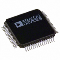
ADV7311KST Analog Devices Inc, ADV7311KST Datasheet - Page 31

ADV7311KST
Manufacturer Part Number
ADV7311KST
Description
IC VID ENC 6-12BIT DAC'S 64LQFP
Manufacturer
Analog Devices Inc
Type
Video Encoderr
Datasheet
1.ADV7311KST.pdf
(84 pages)
Specifications of ADV7311KST
Rohs Status
RoHS non-compliant
Applications
DVD, SD/HD
Voltage - Supply, Analog
2.5V
Voltage - Supply, Digital
2.5V
Mounting Type
Surface Mount
Package / Case
64-LQFP
Input Format
Digital
Output Format
Analog
Supply Voltage Range
2.375V To 2.625V
Operating Temperature Range
0°C To +70°C
Tv / Video Case Style
LQFP
No. Of Pins
64
Msl
MSL 1 - Unlimited
Lead Free Status / RoHS Status
Lead free / RoHS Compliant
Available stocks
Company
Part Number
Manufacturer
Quantity
Price
Company:
Part Number:
ADV7311KST
Manufacturer:
ADI
Quantity:
300
Company:
Part Number:
ADV7311KST
Manufacturer:
Analog Devices Inc
Quantity:
10 000
Part Number:
ADV7311KSTZ
Manufacturer:
ADI/亚德诺
Quantity:
20 000
If in simultaneous SD/HD input mode the two clock phases
differ by less than 9.25 ns or more than 27.75 ns, the CLOCK
ALIGN bit [Address 01h Bit 3] must be set accordingly. If the
application uses the same clock source for both SD and PS, the
CLOCK ALIGN bit must be set since the phase difference
between both inputs is less than 9.25 ns.
Progressive Scan at 27 MHz (Dual Edge) or 54 MHz
Address[01h] : Input Mode 100 or 111, Respectively
YCrCb progressive scan data can be input at 27 MHz or 54 MHz.
The input data is interleaved onto a single 8-/10-bit bus and is
input on Pins Y9–Y0. When a 27 MHz clock is supplied, the data
is clocked in on the rising and falling edge of the input clock and
CLOCK EDGE [Address 0x01, Bit 1] must be set accordingly.
The following figures show the possible conditions: (a) Cb data
on the rising edge and (b) Y data on the rising edge.
REV. A
CLKIN_A
CLKIN_B
Figure 26. Clock Phase with Two Input Clocks
Figure 25. Simultaneous HD and SD Input
t
t
DELAY
DELAY
DECODER
DECODER
SDTV
HDTV
9.25ns OR
27.75ns
1080i
720p
OR
YCrCb
Y
74.25MHz
CrCb
27MHz
10
10
10
3
3
S_VSYNC
S_HSYNC
S_BLANK
CLKIN_A
S[9:0]
C[9:0]
Y[9:0]
P_VSYNC
P_HSYNC
P_BLANK
CLKIN_B
ADV7310/
ADV7311
–31–
Table I provides an overview of all possible input configurations.
PIXEL INPUT
WITH A 54 MHz CLOCK, THE DATA IS LATCHED ON EVERY RISING EDGE.
CLKIN_B
CLOCK EDGE ADDRESS 0x00 BIT 1 SHOULD BE SET TO 0 IN THIS CASE.
CLKIN_B
CLOCK EDGE ADDRESS 0x00 BIT 1 SHOULD BE SET TO 1 IN THIS CASE.
Y9–Y0
Y9–Y0
Figure 27a. Input Sequence in PS Bit Interleaved
Mode (EAV/SAV)
Figure 27b. Input Sequence in PS Bit Interleaved
Mode (EAV/SAV)
CLKIN
Figure 27c. Input Sequence in PS Bit Interleaved
Mode (EAV/SAV)
DATA
Figure 28. 1
3FF
3FF
PROGRESSIVE
DECODER
INTERLACED
3FF
MPEG2
YCrCb
TO
00
00
00
10-Bit PS at 27 MHz or 54 MHz
27MHz OR 54MHz
00
00
YCrCb
00
ADV7310/ADV7311
XY
XY
10
XY
3
Cb0
Y0
CLKIN_A
Y[9:0]
P_VSYNC
P_HSYNC
P_BLANK
ADV7310/
ADV7311
Cb0
Cb0
Y0
Y0
Cr0
Y1
Cr0
Cr0
Y1
Y1


