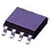
ATTINY12-8SU Atmel, ATTINY12-8SU Datasheet - Page 54

ATTINY12-8SU
Manufacturer Part Number
ATTINY12-8SU
Description
Microcontrollers (MCU) AVR 1K FLASH 64B EE 5V 8MHZ
Manufacturer
Atmel
Datasheet
1.ATTINY12-8SU.pdf
(94 pages)
Specifications of ATTINY12-8SU
Processor Series
ATTINY1x
Core
AVR8
Data Bus Width
8 bit
Program Memory Type
Flash
Program Memory Size
1 KB
Maximum Clock Frequency
8 MHz
Number Of Programmable I/os
6
Number Of Timers
1
Maximum Operating Temperature
+ 85 C
Mounting Style
SMD/SMT
Package / Case
SOIC
3rd Party Development Tools
EWAVR, EWAVR-BL
Development Tools By Supplier
ATAVRDRAGON, ATSTK500
Minimum Operating Temperature
- 40 C
Cpu Family
ATtiny
Device Core
AVR
Device Core Size
8b
Frequency (max)
8MHz
Interface Type
SPI
# I/os (max)
6
Number Of Timers - General Purpose
1
Operating Supply Voltage (typ)
5V
Operating Supply Voltage (max)
5.5V
Operating Supply Voltage (min)
4V
Instruction Set Architecture
RISC
Operating Temp Range
-40C to 85C
Operating Temperature Classification
Industrial
Mounting
Surface Mount
Pin Count
8
Package Type
SOIC EIAJ
Lead Free Status / Rohs Status
Details
Available stocks
Company
Part Number
Manufacturer
Quantity
Price
Company:
Part Number:
ATTINY12-8SU
Manufacturer:
ATMEL
Quantity:
5
High-voltage Serial
Programming
Characteristics
Low-voltage Serial
Downloading (ATtiny12
only)
54
ATtiny11/12
Figure 28. High-voltage Serial Programming Timing
Table 24. High-voltage Serial Programming Characteristics T
5.0V ± 10% (Unless otherwise noted)
Both the program and data memory arrays can be programmed using the SPI bus while
RESET is pulled to GND. The serial interface consists of pins SCK, MOSI (input) and
MISO (output), see Figure 29. After RESET is set low, the Programming Enable instruc-
tion needs to be executed first before program/erase instructions can be executed.
Figure 29. Serial Programming and Verify
t
WLWH_PFB
Symbol
t
t
t
t
t
SHOV
SHSL
SLSH
IVSH
SHIX
Parameter
SCI (PB3) Pulse Width High
SCI (PB3) Pulse Width Low
SDI (PB0), SII (PB1) Valid to SCI (PB3) High
SDI (PB0), SII (PB1) Hold after SCI (PB3) High
SCI (PB3) High to SDO (PB2) Valid
Wait after Instr. 3 for Write Fuse Bits
GND
SDI (PB0), SII (PB1)
SDO (PB2)
SCI (PB3)
GND
PB5 (RESET)
t
IVSH
ATtiny12
t
SHSL
t
SHOV
VCC
PB2
PB1
PB0
t
SHIX
2.2 - 5.5V
Min
100
100
1.7
10
50
50
t
SLSH
A
SCK
MISO
MOSI
= 25°C ± 10%, V
Typ
2.5
16
Max
1006F–AVR–06/07
3.4
32
Units
ms
ns
ns
ns
ns
ns
CC
=


