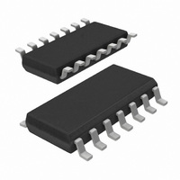
TJA1055T,512 NXP Semiconductors, TJA1055T,512 Datasheet - Page 8

TJA1055T,512
Manufacturer Part Number
TJA1055T,512
Description
IC CAN TXRX FAULT-TOL 14-SOIC
Manufacturer
NXP Semiconductors
Type
Transceiverr
Datasheet
1.TJA1055T3C518.pdf
(26 pages)
Specifications of TJA1055T,512
Package / Case
14-SOIC (3.9mm Width), 14-SOL
Number Of Drivers/receivers
1/1
Protocol
CAN
Voltage - Supply
4.75 V ~ 5.25 V
Mounting Type
Surface Mount
Product
Controller Area Network (CAN)
Number Of Transceivers
1
Data Rate
125 KBd
Supply Voltage (max)
5.25 V, 40 V
Supply Voltage (min)
4.75 V, 5 V
Supply Current (max)
0.22 mA, 21 mA
Maximum Operating Temperature
+ 125 C
Minimum Operating Temperature
- 40 C
Mounting Style
SMD/SMT
Lead Free Status / RoHS Status
Lead free / RoHS Compliant
Other names
935280277512
TJA1055T
TJA1055T
TJA1055T
TJA1055T
NXP Semiconductors
TJA1055_4
Product data sheet
7.3 Power-on
7.4 Protections
A local wake-up through pin WAKE is detected by a rising or falling edge with a
consecutive level exceeding the maximum specified t
On a wake-up request the transceiver will set the output on pin INH to HIGH which can be
used to activate the external supply voltage regulator.
A wake-up request is signalled on ERR or RXD with an active LOW signal. So the external
microcontroller can activate the transceiver (switch to normal operating mode) via
pins STB and EN.
To prevent a false remote wake-up due to transients or RF fields, the wake-up voltage
levels have to be maintained for a certain period of time. In the low power modes the
failure detection circuit remains partly active to prevent an increased power consumption
in the event of failures 3, 3a, 4 and 7.
To prevent a false local wake-up during an open wire at pin WAKE, this pin has a weak
pull-up current source towards V
any EMC immunity issues, it is recommended to connect a not used pin WAKE to pin
BAT. Pin INH is set to floating only if the goto-sleep command is entered successfully. To
enter a successful goto-sleep command under all conditions, this command must be kept
stable for the maximum specified t
Pin INH will be set to a HIGH level again by the following events only:
To provide fail-safe functionality, the signals on pins STB and EN will internally be set to
LOW when V
can simply be left open within the application.
After power-on (V
power-on flag will be set. This flag can be read in the power-on standby mode through
pin ERR (STB = 1; EN = 0) and will be reset by entering the normal operating mode.
A current limiting circuit protects the transmitter output stages against short-circuit to
positive and negative battery voltage.
If the junction temperature exceeds the typical value of 175 C, the transmitter output
stages are disabled. Because the transmitter is responsible for the major part of the power
dissipation, this will result in a reduced power dissipation and hence a lower chip
temperature. All other parts of the device will continue to operate.
The pins CANH and CANL are protected against electrical transients which may occur in
an automotive environment.
•
•
•
•
V
Rising or falling edge on pin WAKE
A message frame with a dominant phase of at least the maximum specified t
or t
Pin STB goes to a HIGH level with V
BAT
dom(CANL)
power-on (cold start)
CC
, while pin EN or pin STB is at a LOW level
is below a certain threshold voltage (V
BAT
switched on) the signal on pin INH will become HIGH and an internal
Rev. 04 — 17 February 2009
BAT
d(sleep)
. However, in order to protect the transceiver against
.
CC
active
Enhanced fault-tolerant CAN transceiver
WAKE
CC(stb)
.
). An unused output pin INH
© NXP B.V. 2009. All rights reserved.
TJA1055
dom(CANH)
8 of 26


