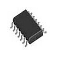
CLC014AJE National Semiconductor, CLC014AJE Datasheet - Page 12

CLC014AJE
Manufacturer Part Number
CLC014AJE
Description
07B4822
Manufacturer
National Semiconductor
Specifications of CLC014AJE
Ic Function
Adaptive Cable Equalizer
Supply Voltage Range
4.5V To 5.5V
Operating Temperature Range
-40°C To +85°C
Digital Ic Case Style
SOIC
No. Of Pins
14
Termination Type
SMD
Rohs Compliant
No
Filter Terminals
SMD
Data Rate Max
650Mbps
Lead Free Status / Rohs Status
Not Compliant
Available stocks
Company
Part Number
Manufacturer
Quantity
Price
Company:
Part Number:
CLC014AJE
Manufacturer:
NS
Quantity:
5 000
Part Number:
CLC014AJE
Manufacturer:
NS/国半
Quantity:
20 000
Company:
Part Number:
CLC014AJE-TR13
Manufacturer:
NS
Quantity:
20
Company:
Part Number:
CLC014AJE/NOPB
Manufacturer:
NSC
Quantity:
772
www.national.com
Layout and Measurement
The printed circuit board layout for the CLC014 requires
proper high-speed layout to achieve the performance speci-
fications found in the datasheet. The following list contains a
few rules to follow:
1. Use a ground plane.
2. Decouple power pins with 0.1 µF capacitors placed
3. Design transmission strip lines from the CLC014’s input
4. Route outputs away from inputs.
5. Keep ground plane ≥ 0.025” (0.06mm) away from the
Troubleshooting with scope probes can affect the equaliza-
tion. For high data rates, use a low capacitance probe with
less than 2 pF probe capacitance. Evaluation boards and
literature are available for quick prototyping and evaluation
of the CLC014 Adaptive Cable Equalizer. The CLC014 con-
tains CMOS devices and operators should use grounding
straps when handling the parts.
Figure 9 shows the CLC014’s internal power supply routing.
Bypass V
• Monolithic capacitor of about 0.1 µF placed less than 0.1”
• Tantalum capacitor of about 6.8 µF for large current
(3mm) from the pin
signal swings placed as close as convenient to the
CLC014
≤ 0.1” (3mm) from the power pins.
and output pins to the board connectors.
input and output pads.
CC
(pin 4) by:
FIGURE 8. Typical Measurement Block
10005628
12
Figure 8 shows a block level measurement diagram, while
Figure 15 on depicts a detailed schematic. A pseudo-random
pattern generator with low output jitter was used to provide a
NRZI pattern to create the eye diagrams shown in the Typi-
cal Performance Characteristics section.
Since most pattern generators have a 50Ω output imped-
ance, a translation can be accomplished using a CLC006
Cable Driver as an impedance transformer. A wide band-
width oscilloscope is needed to observe the high data rate
eye pattern. When monitoring a single output that is termi-
nated at both the equalizer output and the oscilloscope, the
effective output load is 37.5Ω. Consequently, the signal
swing is half that observed for a single-ended 75Ω
termination.
FIGURE 9. Power Package Routing Fixture
10005629


