SCAN92LV090SLC/NOPB National Semiconductor, SCAN92LV090SLC/NOPB Datasheet - Page 6
SCAN92LV090SLC/NOPB
Manufacturer Part Number
SCAN92LV090SLC/NOPB
Description
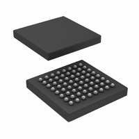
IC TXRX LVDS 9CH W/SCAN 64FBGA
Manufacturer
National Semiconductor
Series
SCANr
Type
Transceiverr
Datasheet
1.SCAN92LV090VEHNOPB.pdf
(14 pages)
Specifications of SCAN92LV090SLC/NOPB
Number Of Drivers/receivers
9/9
Protocol
IEEE 1149.1
Voltage - Supply
3 V ~ 3.6 V
Mounting Type
Surface Mount
Package / Case
64-FBGA
Lead Free Status / RoHS Status
Lead free / RoHS Compliant
Other names
*SCAN92LV090SLC
*SCAN92LV090SLC/NOPB
SCAN92LV090SLC
*SCAN92LV090SLC/NOPB
SCAN92LV090SLC
Available stocks
Company
Part Number
Manufacturer
Quantity
Price
Company:

Part Number:
SCAN92LV090SLC/NOPB
Manufacturer:
Texas Instruments
Quantity:
10 000


www.national.com
t
t
t
t
t
t
t
t
t
t
t
SCAN CIRCUITRY TIMING REQUIREMENTS
f
t
t
t
t
t
t
t
PHLD
PLHD
SDK1
SDK2
SDK3
TLH
THL
PHZ
PLZ
PZH
PZL
MAX
S
H
S
H
W
W
REC
Symbol
Note 1: “Absolute Maximum Ratings” are those values beyond which the safety of the device cannot be guaranteed. They are not meant to imply that the devices
should be operated at these limits. The table of “Electrical Characteristics” provides conditions for actual device operation.
Note 2: All currents into device pins are positive; all currents out of device pins are negative. All voltages are referenced to ground unless otherwise specified
except V
Note 3: All typicals are given for V
Note 4: ESD Rating: HBM (1.5 kΩ, 100 pF) > 4.5 kV EIAJ (0Ω, 200 pF) > 300V.
Note 5: C
Note 6: Generator waveforms for all tests unless otherwise specified: f = 25 MHz, Z
minimum skew, data input edge rates should be equal to or faster than 1ns/V; control signals equal to or faster than 3ns/V. In general, the faster the input edge
rate, the better the AC performance.
Note 7: The DS92LV090A functions within datasheet specification when a resistive load is applied to the driver outputs.
Note 8: Propagation delays are guaranteed by design and characterization.
Note 9: t
Note 10: Only one output at a time should be shorted, do not exceed maximum package power dissipation capacity.
Note 11: V
Note 12: Chip to Chip skew is the difference in differential propagation delay between any channels of any devices, either edge.
Note 13: Channel to Channel skew is the difference in driver output or receiver output propagation delay between any channels within a device, common edge.
OD
SKD1
L
OH
, ΔV
includes probe and fixture capacitance.
Differential Prop. Delay High to Low (Note 8)
Differential Prop Delay Low to High (Note 8)
Differential Skew |t
Chip to Chip Skew (Note 12)
Channel to Channel skew (Note 13)
Transition Time Low to High
Transition Time High to Low
Disable Time High to Z
Disable Time Low to Z
Enable Time Z to High
Enable Time Z to Low
Maximum TCK Clock Frequency
TDI to TCK, H or L
TDI to TCK, H or L
TMS to TCK, H or L
TMS to TCK, H or L
TCK Pulse Width, H or L
TRST Pulse Width, L
Recovery Time, TRST to TCK
|t
failsafe terminated test performed with 27Ω connected between RI+ and RI− inputs. No external voltage is applied.
PHLD
OD
and V
–t
PLHD
ID
| is the worse case skew between any channel and any device over recommended operation conditions.
.
CC
PHLD
= +3.3V and T
–t
Parameter
PLHD
| (Note 9)
A
= +25°C, unless otherwise stated.
6
O
= 50Ω, t
Figure 6, Figure 7
C
R
Figure 8, Figure 9
C
R
L
L
L
L
r
= 35 pF
= 500Ω,
= 35 pF
= 500Ω, C
, t
f
Conditions
= <1.0 ns (0%–100%). To ensure fastest propagation delay and
L
= 35 pF
25.0
10.0
Min
2.0
2.0
1.5
1.5
2.5
1.5
2.5
2.0
0.35
75.0
Typ
210
2.4
2.4
1.5
1.5
4.5
3.5
3.5
3.5
Max
3.9
3.9
1.9
0.7
2.5
2.5
10
8
8
8
MHz
Unit
ns
ns
ps
ns
ns
ns
ns
ns
ns
ns
ns
ns
ns
ns
ns
ns
ns
ns
s
Related parts for SCAN92LV090SLC/NOPB
Image
Part Number
Description
Manufacturer
Datasheet
Request
R

Part Number:
Description:
National Semiconductor [8-Bit D/A Converter]
Manufacturer:
National Semiconductor
Datasheet:
Part Number:
Description:
National Semiconductor [Media Coprocessor]
Manufacturer:
National Semiconductor
Datasheet:
Part Number:
Description:
Digitally Controlled Tone and Volume Circuit with Stereo Audio Power Amplifier, Microphone Preamp Stage and National 3D Sound
Manufacturer:
National Semiconductor
Datasheet:
Part Number:
Description:
Digitally Controlled Tone and Volume Circuit with Stereo Audio Power Amplifier, Microphone Preamp Stage and National 3D Sound
Manufacturer:
National Semiconductor
Datasheet:
Part Number:
Description:
AC97 Rev 2 Codec with Sample Rate Conversion and National 3D Sound
Manufacturer:
National Semiconductor
Part Number:
Description:
Manufacturer:
National Semiconductor
Datasheet:
Part Number:
Description:
Manufacturer:
National Semiconductor
Datasheet:
Part Number:
Description:
General Purpose, Low Voltage, Low Power, Rail-to-Rail Output Operational Amplifiers
Manufacturer:
National Semiconductor
Datasheet:
Part Number:
Description:
8-bit 20 MSPS flash A/D converter.
Manufacturer:
National Semiconductor
Datasheet:
Part Number:
Description:
Low Noise Quad Operational Amplifier
Manufacturer:
National Semiconductor
Datasheet:
Part Number:
Description:
Quad Differential Line Receivers
Manufacturer:
National Semiconductor
Datasheet:
Part Number:
Description:
Quad High Speed Trapezoidal? Bus Transceiver
Manufacturer:
National Semiconductor
Datasheet:
Part Number:
Description:
Dual Line Receiver
Manufacturer:
National Semiconductor
Datasheet:
Part Number:
Description:
TTL to 10k ECL Level Translator with Latch
Manufacturer:
National Semiconductor
Datasheet: