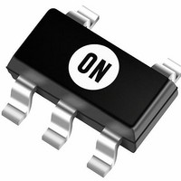
NCP346SN2T1G ON Semiconductor, NCP346SN2T1G Datasheet

NCP346SN2T1G
Specifications of NCP346SN2T1G
Available stocks
Related parts for NCP346SN2T1G
NCP346SN2T1G Summary of contents
Page 1
... ORDERING INFORMATION Device Package Shipping NCP346SN1T1G SOT−23−5 3000 / Tape & Reel (Pb−Free) (7 inch Reel) NCP346SN2T1G †For information on tape and reel specifications, including part orientation and tape sizes, please refer to our Tape and Reel Packaging Specifications Brochure, BRD8011/D. Schottky Diode P−CH ...
Page 2
IN ( Pre−regulator R1 R2 Bandgap Reference CNTRL (3) PIN FUNCTION DESCRIPTIONS Pin # Symbol 1 OUT This signal drives the gate of a P−channel MOSFET controlled by the voltage level the logic ...
Page 3
MAXIMUM RATINGS (T = 25°C unless otherwise noted.) A Rating OUT Voltage to GND Input and CNTRL Pin Voltage to GND Input Pin Voltage Maximum Range CC Maximum Power Dissipation 85°C A Thermal ...
Page 4
ELECTRICAL CHARACTERISTICS (NCP346SN1T1) (For typical values T = 25°C, for min/max values T A Characteristic V Operating Voltage Range CC Total Supply Current (IN Connected CNTRL Pin Floating, Steady State) Total Supply Current (IN Connected to V ...
Page 5
ELECTRICAL CHARACTERISTICS (NCP346SN2T1) (For typical values T = 25°C, for min/max values T A Characteristic V Operating Voltage Range CC Total Supply Current (IN Connected CNTRL Pin Floating, Steady State) Total Supply Current (IN Connected to V ...
Page 6
AC/DC Adapter or Accessory Charger (optional) IN Zener (opt.) Diode (optional) GND Introduction In many electronic products, an external AC/DC wall adapter is used to convert the AC line voltage into a regulated DC voltage or a current limited source. ...
Page 7
... V, therefore, one must ensure that: Where 0.5 = V(V Therefore, the NCP346 should only be adjusted to maximum overvoltage thresholds which are less than greater thresholds are desired than can be accommodated does play the NCP346, ON Semiconductor offers the NCP345 which can withstand those voltages (eq http://onsemi ...
Page 8
Design Steps for Adjusting the Overvoltage Threshold 1. Use Typical R , and V Values from the Electrical in th Specifications 2. Minimize R Effect by Selecting ...
Page 9
Table 1. Design Steps 1−5 Parameter IN Pin Input Impedance ( Input Threshold ( Ratio ( Desired Overvoltage Threshold ( Table 2. Design Steps ...
Page 10
Vth (V Increasing) CC 4.45 Vth (V Decreasing) CC 4.4 4.35 4.3 −40 −25 − AMBIENT TEMPERATURE (°C) Figure 5. Typical Vth Variation vs. Temperature (NCP346SN1) 900 800 Overvoltage Tripped ( ...
Page 11
AMBIENT TEMPERATURE (°C) Figure 11. Typical OUT Sink Current vs. Temperature (NCP346SN1) NCP346 ...
Page 12
NCP346 V CNTRL V Load Figure 13. Typical Turn−off Time CNTRL (NCP346SN1) V CNTRL V Load Figure 14. Typical Turn−off Time CNTRL (NCP346SN2) http://onsemi.com 12 MOSFET = NTHS4101PT1 C1= N/C Load = 50 W (See Figure 3) MOSFET = NTHS4101PT1 ...
Page 13
NCP346 V CNTRL V Load Figure 15. Typical Turn−on Time CNTRL (NCP346SN1) V CNTRL V Load Figure 16. Typical Turn−on Time CNTRL (NCP346SN2) http://onsemi.com 13 MOSFET = NTHS4101PT1 C1 = N/C Load = 50 W (See Figure 3) MOSFET = ...
Page 14
The power dissipation of the Thin SOT−23− function of the pad size. This can vary from the minimum pad size for soldering to a pad size given for maximum power dissipation. Power dissipation for a surface mount device ...
Page 15
... H *For additional information on our Pb−Free strategy and soldering details, please download the ON Semiconductor Soldering and Mounting Techniques Reference Manual, SOLDERRM/D. ON Semiconductor and are registered trademarks of Semiconductor Components Industries, LLC (SCILLC). SCILLC reserves the right to make changes without further notice to any products herein ...


