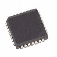
DS3150Q+ Maxim Integrated Products, DS3150Q+ Datasheet - Page 19

DS3150Q+
Manufacturer Part Number
DS3150Q+
Description
IC LIU T3/E3/STS-1 28-PLCC
Manufacturer
Maxim Integrated Products
Type
Line Interface Units (LIUs)r
Datasheet
1.DS3150T.pdf
(28 pages)
Specifications of DS3150Q+
Number Of Drivers/receivers
1/1
Protocol
DS3
Voltage - Supply
3.135 V ~ 3.465 V
Mounting Type
Surface Mount
Package / Case
28-LCC, 28-PLCC
Lead Free Status / RoHS Status
Lead free / RoHS Compliant
Note 1:
Note 2:
Note 3:
NAME
OFSEL
TDS1/
TNEG
TPOS/
TNRZ
TESS
ZCSE
TX+,
TTS
TX-
V
V
DD
SS
Pin type I = input pin. Pin type O = output pin. Pin type P = power-supply pin.
Pin type I3 is an input capable of detecting three states: high, low, and float. All I3 inputs have an internal 13kW pullup to
approximately 1.5V. The voltage range of the float state is approximately 1.2V to 1.9V. If the function of the float state of an I3 pin
is not defined in
Pin type O3 is an output that is tri-state capable.
(Note 2)
(Note 2)
(Note 2)
(Note 2)
(Note 3)
TYPE
O3
I3
I3
I3
I3
P
P
I
I
Table
Transmit Data Select Bit 1/Oscillator Frequency Select. If EFE = 1, TDS1, TDS0
and TESS select the source of the transmit data
ignored. If MCLK is wired low, TDS1 is internally pulled low, and a resistor connected
between this pin (OFSEL) and ground determines the frequency of an internal
oscillator. The following resistor values should be used for specific applications:
E3: 6.81kW, ±2%
DS3: 5.23kW, ±2%
STS-1: 4.53kW, ±2%
When switching among DS3, E3, and STS-1 modes, do not allow OFSEL to float.
Instead, hardwire the highest resistor value and switch in series or parallel resistors as
needed. Example: For a DS3/E3 application, hardwire 5.23kΩ for DS3 and switch in
series 1.58kΩ to get 6.81kΩ for E3.
T3/E3/STS-1 Select. TESS determines the mode of operation for the device.
0 = E3
1 = T3 (DS3)
Float = STS-1
Transmit Negative Data. When the B3ZS/HDB3 encoder is disabled (ZCSE = 1),
TNEG should be driven high to transmit a negative AMI pulse. When the B3ZS/HDB3
encoder is enabled (ZCSE = 0), the NRZ data stream should be applied to TNRZ, while
TNEG is ignored and can be wired either high or low. TNEG is sampled either on the
falling edge of TCLK (ICE = 1 or Float) or the rising edge of TCLK (ICE = 0).
Transmit Positive Data. When the B3ZS/HDB3 encoder is disabled (ZCSE = 1),
TPOS should be driven high to transmit a positive AMI pulse. When the B3ZS/HDB3
encoder is enabled (ZCSE = 0), the NRZ data stream should be applied to TNRZ.
TPOS/TNRZ is sampled either on the falling edge of TCLK (ICE = 1 or Float) or the
rising edge of TCLK (ICE = 0).
Transmit Tri-State. TTS determines whether the TX+ and TX- analog outputs are tri-
stated or active. This input also controls the jitter attenuator
0 = tri-state the transmit output driver, disable the jitter attenuator in the transmit path
1 = enable the transmit output driver, disable the jitter attenuator in the transmit path
Float = enable the transmit output driver, enable the jitter attenuator in the transmit path
Transmit Analog Outputs. These differential AMI outputs are coupled to the
outbound 75W coaxial cable through a 2:1 step-down transformer
outputs can be tri-stated using the TTS input pin.
Positive Supply. 3.3V ±5%. All V
Ground Reference. All V
Active-Low Zero Code Suppression Enable. ZCSE has an internal 80kW pullup to
V
0 = B3ZS/HDB3 encoder/decoder enabled (NRZ interface enabled)
1 = B3ZS/HDB3 encoder/decoder disabled (bipolar interface enabled)
DD
2-A, then the float state is used for factory test only.
.
SS
19 of 28
pins should be wired together.
DD
FUNCTION
pins should be wired together.
(Table
2-B). If EFE = 0, TDS1 is
(Table
(Figure
2-C).
1-2). These


