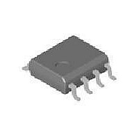
FAN3278TMX Fairchild Semiconductor, FAN3278TMX Datasheet - Page 7

FAN3278TMX
Manufacturer Part Number
FAN3278TMX
Description
MOSFET & Power Driver ICs Low-Voltage 27V PMOS NMOS Bridge Driver
Manufacturer
Fairchild Semiconductor
Datasheet
1.FAN3278TMX.pdf
(15 pages)
Specifications of FAN3278TMX
Product
MOSFET Gate Drivers
Rise Time
17 ns
Fall Time
8 ns
Propagation Delay Time
45 ns
Supply Voltage (max)
27 V
Supply Current
1.3 mA
Mounting Style
SMD/SMT
Package / Case
SOIC-8
Output Current
1.5 A
Output Voltage
30 V
Lead Free Status / Rohs Status
Lead free / RoHS Compliant
Available stocks
Company
Part Number
Manufacturer
Quantity
Price
Company:
Part Number:
FAN3278TMX
Manufacturer:
PANASONIC
Quantity:
12 000
Part Number:
FAN3278TMX
Manufacturer:
FAIRCHILD/仙童
Quantity:
20 000
© 2010 Fairchild Semiconductor Corporation
FAN3278 • Rev. 1.0.0
Electrical Characteristics
Unless otherwise noted, V
negative out of the device (I
Output
Notes:
8.
9.
10. Not tested in production.
11. See the Timing Diagrams of Figure 5 and Figure 6.
Symbol
R
R
R
R
I
I
V
V
V
V
O_A_SINK
O_B_SINK
O_A_SRC
O_B_SRC
PK_OFF
t
t
PK_ON
t
t
I
OFF,N
OFF,P
I
ON,N
I
ON,P
OUTA
OUTB
OUTA
OUTB
t
t
OFF
RVS
ON
D1
D2
The internal gate-drive regulators provide optimum gate-drive voltage when operating from a rail of 8V to 27V.
The FAN3278 can be driven from a voltage rail of less than 8V; however, with reduced gate drive current.
EN inputs have near-TTL thresholds (refer to the ENABLE section).
OUT Current, Peak, Turn-Off
OUT Current, Peak, Turn-On
OUT Current, Mid-Voltage, Turn-Off
OUT Current, Mid-Voltage, Turn-On
OUTA Drive Voltage
OUTB Drive Voltage, V
OUTA Drive Voltage
OUTB Drive Voltage, V
OUTA Sink Impedance (Turn-Off)
OUTA Source Impedance (Turn-On)
OUTB Sink Impedance (Turn-On)
OUTB Source Impedance (Turn-Off)
Output A Rise Time
Output A Fall Time
Output B Fall Time
Output B Rise Time
Output Propagation Delay On
Output Propagation Delay Off
Output Reverse Current Withstand
Parameter
DD
source
=12V and T
(11)
(11)
(11)
(11)
).
DD
DD
(Continued)
– V
– V
J
(10)
(10)
=-40°C to +125°C. Currents are defined as positive into the device (I
OUTB
OUTB
(11)
(11)
(10)
(10)
(10)
(10
(10)
(10)
(10)
C
C
OUT at V
f=1kHz
OUT at V
f=1kHz
V
V
V
V
V
V
V
V
C
C
C
C
0 - 5V
0 - 5V
DD
DD
DD
DD
DD
DD
DD
DD
LOAD
LOAD
LOAD
LOAD
LOAD
LOAD
=27V, INA=“HI”
=27V, INA=“HI”
=10V, INB=“HI”
=10V, INB=“HI”
=6V, C
=6V, C
=6V, C
=6V, C
7
=0.1µF, f=1kHz
=0.1µF, f=1kHz
=1000pF to GND
=1000pF to GND
=1000pF to V
=1000pF to V
IN
IN
, 1V/ns Slew Rate
, 1V/ns Slew Rate
Conditions
DD
DD
LOAD
LOAD
LOAD
LOAD
, C
/2, C
LOAD
=0.1µF
=0.1µF
=0.1µF
=0.1µF
LOAD
=0.1µF,
DD
DD
=0.1µF,
Min.
6.5
6.5
Typ. Max.
10.3
13.7
-1.0
-0.5
500
1.5
1.0
7.0
7.0
4.2
6.8
11
11
17
21
45
35
8
8
13
13
30
15
30
15
70
60
www.fairchildsemi.com
sink
) and
Unit
mA
ns
ns
ns
ns
ns
ns
Ω
Ω
Ω
Ω
A
A
A
A
V
V
V
V


