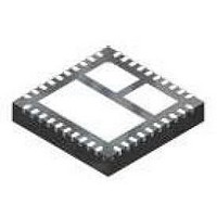
FDMF6705 Fairchild Semiconductor, FDMF6705 Datasheet

FDMF6705
Specifications of FDMF6705
Available stocks
Related parts for FDMF6705
FDMF6705 Summary of contents
Page 1
... MOSFET plus driver power stage solutions for high-current, high- frequency, synchronous buck DC-DC applications. The FDMF6705 integrates a driver IC, two power MOSFETs, and a bootstrap Schottky diode into a thermally enhanced, ultra-compact 6x6mm PQFN package. With an integrated approach, the complete switching ...
Page 2
... Typical Application Circuit VDRV DISB# PWM Input OFF ON Open-Drain Output DrMOS Block Diagram © 2011 Fairchild Semiconductor Corporation FDMF6705 • Rev. 1.0.1 VDRV VCIN VIN R BOOT DISB# BOOT PWM FDMF6705 PHASE SMOD# VSWH THWN# PGND CGND Figure 1. Typical Application Circuit Figure 2. ...
Page 3
... LOW). This pin has a 10µA internal pull-down current source. Do not leave this pin floating. Do not add a noise filter capacitor. 40 PWM PWM signal input. This pin accepts a 3-state logic-level PWM signal from the controller. © 2011 Fairchild Semiconductor Corporation FDMF6705 • Rev. 1.0.1 Figure 4. Top View Description 3 www.fairchildsemi.com ...
Page 4
... MOSFET switching transients. For reliable DrMOS operation, VSWH to GND and BOOT to GND must remain at or below the Absolute Maximum Ratings. Refer to the Application Information and PCB Layout Guidelines sections of this datasheet for more information. © 2011 Fairchild Semiconductor Corporation FDMF6705 • Rev. 1.0.1 Parameter f =300kHz ...
Page 5
... High-Level Input Voltage IH_SMOD V Low-Level Input Voltage IL_SMOD I Pull-Up Current PLU t Propagation Delay PD_SLGLL t Propagation Delay PD_SHGLH © 2011 Fairchild Semiconductor Corporation FDMF6705 • Rev. 1.0 5V, and T = +25°C unless otherwise noted. CIN DRV A Condition PWM=LOW or HIGH or Float Q VCIN VDRV ...
Page 6
... Exiting 3-State Propagation t PD_TSGLH Delay Boot Diode V Forward-Voltage Drop F V Breakdown Voltage R © 2011 Fairchild Semiconductor Corporation FDMF6705 • Rev. 1.0 5V, and T = +25°C unless otherwise noted. CIN DRV A Condition I =5mA PLD SW=0V, Delay Between GH from HIGH to LOW and GL from LOW to HIGH ...
Page 7
... V IH_PWM PWM PHGLL t D_DEADON © 2011 Fairchild Semiconductor Corporation FDMF6705 • Rev. 1.0.1 90% 1.0V 10 PLGHL Figure 5. PWM Timing Diagram 7 V IL_PWM 10% 90% 1.2V t D_TIMEOUT (250ns Timeout) 2.2V t D_DEADOFF www.fairchildsemi.com ...
Page 8
... Output Current, I Figure 8. Module Power Loss vs. Output Current 1. 30A 300kHz OUT SW 1.15 1.10 1.05 1.00 0. Module Input Voltage, V Figure 10. Normalized Power Loss vs. Input Voltage © 2011 Fairchild Semiconductor Corporation FDMF6705 • Rev. 1.0.1 =1.0V, V =5V, V =5V, L =320nH, T CIN DRV OUT 1MHz ...
Page 9
... Figure 14. Driver Supply Current vs. Frequency 1.10 1.08 1.06 1.04 1.02 1.00 0. Module Output Current, I Figure 16. Normalized Driver Supply Current vs. Output Current © 2011 Fairchild Semiconductor Corporation FDMF6705 • Rev. 1.0.1 (Continued) =1.0V, V =5V, V =5V, L =320nH, T CIN DRV OUT 1.05 1.04 1.03 1.02 1.01 1.00 0.99 ...
Page 10
... Driver Supply Voltage, V Figure 22. DISB# Thresholds vs. Driver Supply Voltage © 2011 Fairchild Semiconductor Corporation FDMF6705 • Rev. 1.0.1 (Continued) =1.0V, V =5V, V =5V, L =320nH, T CIN DRV OUT 2.2 V IH_PWM 2.0 1.8 1.6 ...
Page 11
... V IN OUT unless otherwise specified. 11 CIN 11.0 10.5 10.0 9.5 -50 - Driver IC Junction Temperature, T Figure 24. DISB# Pull-Down Current vs. Temperature © 2011 Fairchild Semiconductor Corporation FDMF6705 • Rev. 1.0.1 (Continued) =1.0V, V =5V, V =5V, L =320nH, T CIN DRV OUT I PLD 50 75 100 125 150 (° =25° ...
Page 12
... LOW, the low side MOSFET is turned on. If the PWM input goes from 3-state to HIGH, the high-side MOSFET is turned on. This is illustrated in Figure 26. The FDMF6705 design allows Driver State for short propagation delays when exiting the 3-state window (see Electrical Characteristics). ...
Page 13
... PD_SHGLH GS © 2011 Fairchild Semiconductor Corporation FDMF6705 • Rev. 1.0.1 voltage at the VSWH pin. When the PWM signal goes LOW, Q1 begins to turn off after some propagation delay (t Q2 begins to turn on after adaptive delay t Additionally, V discharged below ~1 ...
Page 14
... SW 2. 90% 1. PD_PLGHL PD_PHGLL t t D_DEADOFF D_DEADON © 2011 Fairchild Semiconductor Corporation FDMF6705 • Rev. 1.0.1 Table 2. DISB Note: 4. The SMOD feature is intended to have low propagation delay between the SMOD signal and the low-side FET V diode emulation on a cycle-by-cycle basis. V CCM ...
Page 15
... Drain Output Figure 28. Power Loss Measurement Block Diagram © 2011 Fairchild Semiconductor Corporation FDMF6705 • Rev. 1.0.1 VCIN Filter The VDRV pin provides power to the gate drive of the high-side and low-side power MOSFETs. In most cases, VDRV can be connected directly to VCIN, which supplies power to the logic circuitry of the gate driver ...
Page 16
... DrMOS cooling while maintaining acceptable noise emission output inductor should be located close to the FDMF6705 to minimize the power loss due to the VSWH copper trace. Care should also be taken so the inductor dissipation does not heat the DrMOS. 4. PowerTrench® MOSFETs are used in the output stage ...
Page 17
... Top View © 2011 Fairchild Semiconductor Corporation FDMF6705 • Rev. 1.0.1 Figure 30. PCB Layout Example 17 Bottom View www.fairchildsemi.com ...
Page 18
... Package specifications do not expand the terms of Fairchild’s worldwide terms and conditions, specifically the warranty therein, which covers Fairchild products. Always visit Fairchild Semiconductor’s online packaging area for the most recent package drawings: http://www.fairchildsemi.com/packaging/. © 2011 Fairchild Semiconductor Corporation FDMF6705 • Rev. 1.0.1 B PIN#1 INDICATOR 6.00 ...
Page 19
... Fairchild Semiconductor Corporation FDMF6705 • Rev. 1.0.1 19 www.fairchildsemi.com ...


