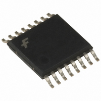
FIN1047MTC Fairchild Semiconductor, FIN1047MTC Datasheet - Page 2

FIN1047MTC
Manufacturer Part Number
FIN1047MTC
Description
IC DRIVER 3.3V LVDS 4BIT 16TSSOP
Manufacturer
Fairchild Semiconductor
Type
Driverr
Datasheet
1.FIN1047MTC.pdf
(9 pages)
Specifications of FIN1047MTC
Number Of Drivers/receivers
4/0
Protocol
LVDS
Voltage - Supply
3 V ~ 3.6 V
Mounting Type
Surface Mount
Package / Case
16-TSSOP
Logic Family
FIN10
Logic Type
High Speed Differential Driver
Supply Voltage (max)
3.6 V
Supply Voltage (min)
3 V
Maximum Operating Temperature
+ 85 C
Mounting Style
SMD/SMT
Data Rate
400 Mbps
Interface
EIA/TIA-644
Minimum Operating Temperature
- 40 C
Number Of Lines (input / Output)
1 / 1
Supply Current
22 mA
Lead Free Status / RoHS Status
Lead free / RoHS Compliant
Available stocks
Company
Part Number
Manufacturer
Quantity
Price
Part Number:
FIN1047MTCX
Manufacturer:
FAIRCHILD/仙童
Quantity:
20 000
www.fairchildsemi.com
V
V
V
V
I
I
V
V
I
I
I
V
I
I
OFF
OS
IN
OZ
I(OFF)
CC
PU/PD
Absolute Maximum Ratings
DC Electrical Characteristics
Over supply voltage and operating temperature ranges, unless otherwise specified
Note 2: All typical values are at T
Note 3: For transient conditions when t
V
V
OD
OS
OH
OL
IH
IL
IK
Symbol
Supply Voltage (V
DC Input Voltage (V
DC Input Voltage (V
Driver Short Circuit Current (I
Storage Temperature Range (T
Max Junction Temperature (T
Lead Temperature (T
ESD (Human Body Model)
ESD (Machine Model)
OD
OS
(Soldering, 10 seconds)
Output Differential Voltage
V
Differential LOW-to-HIGH
Offset Voltage
Offset Magnitude Change from
Differential LOW-to-HIGH
HIGH Output Voltage
LOW Output Voltage
Power Off Output Current
Short Circuit Output Current
Input HIGH Voltage
Input LOW Voltage (Note 3)
Input Current
Disabled Output Leakage Current
Power-Off Input Current
Input Clamp Voltage
Power Supply Current
Output Power Up/Power Down
High Z Leakage Current
OD
Magnitude Change from
CC
IN
OUT
)
L
)
Parameter
)
)
A
25 C and with V
OSD
J
)
STG
5ns and I
)
)
IN
CC
65 C to 150 C
100 mA, V
R
See Figure 1
V
V
V
V
V
V
V
V
I
No Load, V
R
R
V
3.3V.
0.5V to 4.6V
IK
(Note 1)
L
IN
IN
CC
OUT
OD
IN
OUT
CC
L
L
CC
0.5V to 4.6V
0.5V to 6V
Continuous
100 , Driver Enabled,
100 , Driver Disabled
100 , V
V
0V
0V or V
18 mA
0V, V
0V, Driver Enabled
0V, V
0V or 1.5V
CC
0V, Driver Enabled
0V or 4.6V
ILmin
9000V
1200V
150 C
260 C
IN
OUT
IN
CC
Test Conditions
IN
1.0V.
0V or V
0V or 3.6V
0V or V
0V or 3.6V
2
Recommended Operating
Conditions
Note 1: The “Absolute Maximum Ratings”: are those values beyond which
damage to the device may occur. The databook specifications should be
met, without exception, to ensure that the system design is reliable over its
power supply, temperature and output/input loading variables. Fairchild
does not recommend operation of circuits outside databook specification.
Supply Voltage (V
Input Voltage (V
Operating Temperature (T
CC
CC
, Driver Enabled
, Driver Enabled
IN
CC
)
)
1.125
GND
Min
250
0.9
2.0
1.5
20
20
20
20
20
A
)
(Note 2)
1.25
1.05
Typ
340
1.4
1.2
1.4
1.7
16
3.5
0.7
5
3
V
CC
1.375
Max
450
1.6
0.8
40 C to 85 C
25
25
20
20
20
20
22
20
8
4
6
6
3.0V to 3.6V
1.0
0 to V
Units
mV
mV
mV
mA
mA
V
V
V
V
V
V
A
A
A
A
A
CC


