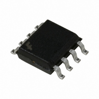
FIN1027AMX Fairchild Semiconductor, FIN1027AMX Datasheet - Page 4

FIN1027AMX
Manufacturer Part Number
FIN1027AMX
Description
IC DRIVER 3.3V LVDS HS 8-SOIC
Manufacturer
Fairchild Semiconductor
Type
Driverr
Datasheet
1.FIN1027AMX.pdf
(11 pages)
Specifications of FIN1027AMX
Number Of Drivers/receivers
2/0
Protocol
LVDS
Voltage - Supply
3 V ~ 3.6 V
Mounting Type
Surface Mount
Package / Case
8-SOIC (3.9mm Width)
Supply Voltage (max)
3.6 V
Supply Voltage (min)
3 V
Maximum Operating Temperature
150 C
Mounting Style
SMD/SMT
Data Rate
600 Mbps
Interface
EIA/TIA-644
Minimum Operating Temperature
- 65 C
Supply Current
12.5 mA
Lead Free Status / RoHS Status
Lead free / RoHS Compliant
Other names
FIN1027AMX
FIN1027AMXTR
FIN1027AMXTR
Available stocks
Company
Part Number
Manufacturer
Quantity
Price
Company:
Part Number:
FIN1027AMX
Manufacturer:
Fairchild
Quantity:
1 358
© 2001 Fairchild Semiconductor Corporation
FIN1027 / FIN1027A • Rev. 1.0.3
DC Electrical Characteristics
All typical values are at T
otherwise noted.
AC Electrical Characteristics
All typical values are at T
otherwise noted.
Notes:
1.
2.
t
SK(LH),
Symbol
Symbol
t
t
are switching in the same direction.
t
devices switching in the same direction (either LOW-to-HIGH or HIGH-to-LOW) when both devices operate with
the same supply voltage, same temperature, and have identical test circuits.
t
t
t
t
t
SK(PP)
ΔV
I
ΔV
C
SK(LH)
SK(PP)
PLHD
PHLD
TLHD
THLD
SK(P)
V
V
I
I(OFF)
C
V
V
I
V
I
OFF
I
OS
CC
OUT
IN
OD
OS
t
IH
IK
IN
IL
OD
OS
SK(HL)
, t
is the magnitude of the difference in propagation delay times between any specified terminals of two
SK(HL)
Differential Propagation Delay,
LOW-to-HIGH
Differential Propagation Delay,
HIGH-to-LOW
Differential Output Rise Time
(20% to 80%)
Differential Output Fall Time
(80% to 20%)
Pulse Skew ⏐t
Channel-to-Channel Skew
Part-to-Part Skew
Output Differential Voltage
V
Differential LOW-to-HIGH
Offset Voltage
Offset Magnitude Change from
Differential LOW-to-HIGH
Power-Off Output current
Short-Circuit Output Current
Input HIGH Voltage
Input LOW Voltage
Input Current
Power-Off Input Current
Input Clamp Voltage
Power Supply Current
Input Capacitance
Output Capacitance
is the skew between specified outputs of a single device when the outputs have identical loads and
OD
Magnitude Change from
A
A
Parameter
= 25°C and V
= 25°C and V
Parameter
PLH -
(2)
t
PHL
⏐
(1)
CC
CC
= 3.3V. Over-supply voltage and operating temperature ranges, unless
= 3.3V. Over-supply voltage and operating temperature ranges, unless
R
V
V
V
V
V
I
No Load, V
R
IK
CC
OUT
OD
IN
CC
L
L
= -18mA
= 100Ω, Figure 4
= 100Ω, V
= 0V or V
= 0V, V
= 0V, V
= 0V
= 0V
R
C
Figure 5, Figure 6
Conditions
4
L
L
= 100Ω,
= 10pF,
Conditions
IN
OUT
IN
CC
IN
= 0V or V
= 0V or 3.6V
= 0V or V
= 0V or 3.6V
CC
CC
Min.
1.125
Min.
GND
250
-1.5
0.5
0.5
0.4
0.4
2.0
1.250
Typ.
Typ.
350
4
6
1.375
Max.
Max.
12.5
17.0
450
±20
V
±20
±20
0.8
1.5
1.5
1.0
1.0
0.5
0.3
1.0
25
25
±8
-8
CC
www.fairchildsemi.com
Units
Units
mV
mV
mV
mA
mA
mA
µA
µA
µA
pF
pF
ns
ns
ns
ns
ns
ns
ns
V
V
V
V


