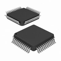
ISL5314IN Intersil, ISL5314IN Datasheet - Page 10
ISL5314IN
Manufacturer Part Number
ISL5314IN
Description
IC SYNTHESIZER DIGITAL 48-MQFP
Manufacturer
Intersil
Datasheet
1.ISL5314INZ.pdf
(17 pages)
Specifications of ISL5314IN
Resolution (bits)
14 b
Master Fclk
125MHz
Tuning Word Width (bits)
48 b
Voltage - Supply
3 V ~ 5.5 V, 4.5 V ~ 5.5 V
Operating Temperature
-40°C ~ 85°C
Mounting Type
Surface Mount
Package / Case
48-LQFP
Peak Reflow Compatible (260 C)
No
Leaded Process Compatible
No
Bus Frequency
48Hz
Rohs Compliant
No
Lead Free Status / RoHS Status
Contains lead / RoHS non-compliant
Available stocks
Company
Part Number
Manufacturer
Quantity
Price

Company:
Part Number:
ISL5314INZ
Manufacturer:
PEREGRIN
Quantity:
2 800


Electrical Specifications
Address Setup Time, t
Address Hold Time, t
UPDATE Pulse Width, t
UPDATE Setup Time, t
UPDATE Hold Time, t
UPDATE Latency, t
UPDATE Latency, t
Maximum PH Rate
Phase Pulse Width, t
Phase Setup Time, t
Phase Hold Time, t
Phase Latency, t
Maximum ENOFR Rate
ENOFR Pulse Width, t
ENOFR Setup Time, t
ENOFR Hold Time, t
ENOFR Latency, t
Write Enable Pulse Width, t
Write Enable Setup Time, t
Write Enable Hold Time, t
RESET Pulse Width, t
RESET Setup Time, t
RESET Latency to Output, t
RESET Latency to Write, t
Maximum SCLK Rate
SCLK Pulse Width, t
SDATA Pulse Width, t
SDATA Setup Time, t
SDATA Hold Time, t
SSYNC Pulse Width, t
SSYNC Setup Time, t
SSYNC Hold Time, t
COMPARATOR CHARACTERISTICS
Input Capacitance
PARAMETER
PL
EL
PH
UL
UL
SDH
PS
SCW
EH
SSH
PW
AH
SDS
RS
UH
SDW
SSS
ES
RW
AS
SSW
EW
US
UW
WH
RE
WS
WR
RL
10
AV
all Min and Max Values. T
temperature range, -40°C to +85°C. (Continued)
DD
Between ADDR and WR (Note 6)
Between ADDR and WR (Note 6)
(Note 6)
Between UPDATE and CLK (Note 6)
Between UPDATE and CLK (Note 6)
After UPDATE, before analog output change, if asserted after
writing to the control registers
After UPDATE, before analog output change, if asserted before
writing to the control registers
Rate of PH1 and PH0 pins (Note 6)
PH(1:0) (Note 6)
Between PH(1:0) change and CLK (Note 6)
Between PH(1:0) change and CLK (Note 6)
Between PH(1:0) change and analog output change
Rate of ENOFR (Note 6)
ENOFR (Note 6)
Between ENOFR and CLK (Note 6)
Between ENOFR and CLK (Note 6)
After ENOFR, before analog output change
WE (Note 6)
Between WE and WR (Note 6)
Between WE and WR (Note 6)
RESET (Note 6)
Between RESET and CLK
After RESET, before analog output reflects reset values
After RESET, before the control registers can be written to
See Figure 6 on page 14 (Note 6)
See Figure 6 on page 14 (Note 6)
See Figure 6 on page 14 (Note 6)
Between SDATA and SCLK. See Figure 6 on page 14. (Note 6)
Between SDATA and SCLK. See Figure 6 on page 14. (Note 6)
See Figure 6 on page 14 (Note 6)
Between SSYNC and SCLK. See Figure 6 on page 14. (Note 6)
Between SSYNC and SCLK. See Figure 6 on page 14. (Note 6)
= DV
DD
= +5V (unless otherwise noted), V
A
TEST CONDITIONS
= +25°C for All Typical Values. Boldface limits apply over the operating
ISL5314
REF
= Internal 1.2V, IOUTFS = 20mA, T
(Note 4)
f
f
CLK
CLK
MIN
12
50
0
5
1
3
5
1
3
5
1
3
5
2
4
5
1
5
5
6
1
5
6
1
-
-
-
-
-
-
-
/2
/2
TYP
14
12
14
11
11
1
4
-
-
-
-
-
-
-
-
-
-
-
-
-
-
-
-
-
-
-
-
-
-
-
-
-
-
A
= -40°C to +85°C for
(Note 4)
MAX
-
-
-
-
-
-
-
-
-
-
-
-
-
-
-
-
-
-
-
-
-
-
-
-
-
-
-
-
-
-
-
-
-
January 19, 2010
UNITS
Cycles
Cycles
Cycles
Cycles
Cycles
Cycles
FN4901.3
MSPS
Clock
Clock
Clock
Clock
Clock
Clock
Hz
Hz
pF
ns
ns
ns
ns
ns
ns
ns
ns
ns
ns
ns
ns
ns
ns
ns
ns
ns
ns
ns
ns
ns
ns
ns
Related parts for ISL5314IN
Image
Part Number
Description
Manufacturer
Datasheet
Request
R

Part Number:
Description:
Intersil Corporation [CMOS Serial Controller Interface]
Manufacturer:
Intersil Corporation
Datasheet:
Part Number:
Description:
Manufacturer:
Intersil Corporation
Datasheet:
Part Number:
Description:
357-036-542-201 CARDEDGE 36POS DL .156 BLK LOPRO
Manufacturer:
Intersil Corporation
Datasheet:
Part Number:
Description:
1024-Word x 4-Bit LSI Static RAM
Manufacturer:
Intersil Corporation
Datasheet:
Part Number:
Description:
General Purpose NPN Transistor Arrays FN341.4
Manufacturer:
Intersil Corporation
Datasheet:
Part Number:
Description:
CMOS 16-Bit Microprocessor
Manufacturer:
Intersil Corporation
Datasheet:
Part Number:
Description:
Manufacturer:
Intersil Corporation
Datasheet:
Part Number:
Description:
Manufacturer:
Intersil Corporation
Datasheet:
Part Number:
Description:
Manufacturer:
Intersil Corporation
Datasheet:
Part Number:
Description:
Manufacturer:
Intersil Corporation
Datasheet:
Part Number:
Description:
CMOS 6-Bit Latch and Decoder Memory Interfaces
Manufacturer:
Intersil Corporation
Datasheet:
Part Number:
Description:
CA3046General Purpose NPN Transistor Arrays
Manufacturer:
Intersil Corporation
Datasheet:
Part Number:
Description:
Manufacturer:
Intersil Corporation
Datasheet:
Part Number:
Description:
TR909 DLC/FLC SLIC with Low Power Standby
Manufacturer:
Intersil Corporation
Datasheet:
Part Number:
Description:
Manufacturer:
Intersil Corporation
Datasheet: