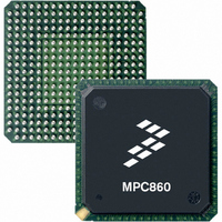
MPC885VR80 Freescale Semiconductor, MPC885VR80 Datasheet - Page 3

MPC885VR80
Manufacturer Part Number
MPC885VR80
Description
IC MPU POWERQUICC 80MHZ 357PBGA
Manufacturer
Freescale Semiconductor
Datasheet
1.MPC880VR80.pdf
(87 pages)
Specifications of MPC885VR80
Processor Type
MPC8xx PowerQUICC 32-Bit
Speed
80MHz
Voltage
3.3V
Mounting Type
Surface Mount
Package / Case
357-PBGA
Processor Series
MPC8xx
Core
MPC8xx
Data Bus Width
32 bit
Maximum Clock Frequency
80 MHz
Maximum Operating Temperature
+ 95 C
Mounting Style
SMD/SMT
Minimum Operating Temperature
0 C
For Use With
CWH-PPC-885XN-VX - BOARD EVAL QUICCSTART MPC885CWH-PPC-885XN-VE - BOARD EVAL QUICCSTART MPC885
Lead Free Status / RoHS Status
Lead free / RoHS Compliant
Features
-
Lead Free Status / Rohs Status
Lead free / RoHS Compliant
Available stocks
Company
Part Number
Manufacturer
Quantity
Price
Company:
Part Number:
MPC885VR80
Manufacturer:
Freescale Semiconductor
Quantity:
135
Company:
Part Number:
MPC885VR80
Manufacturer:
Freescale Semiconductor
Quantity:
10 000
Freescale Semiconductor
•
•
•
•
•
•
•
Provides enhanced ATM functionality found on the MPC862 and MPC866 families and includes
the following:
— Improved operation, administration and maintenance (OAM) support
— OAM performance monitoring (PM) support
— Multiple APC priority levels available to support a range of traffic pace requirements
— Port-to-port switching capability without the need for RAM-based microcode
— Simultaneous MII (100BaseT) and UTOPIA (half- or full -duplex) capability
— Optional statistical cell counters per PHY
— UTOPIA L2-compliant interface with added FIFO buffering to reduce the total cell
— Parameter RAM for both SPI and I
— Supports full-duplex UTOPIA master (ATM side) and slave (PHY side) operations using a split
— AAL2/VBR functionality is ROM-resident
Up to 32-bit data bus (dynamic bus sizing for 8, 16, and 32 bits)
Thirty-two address lines
Memory controller (eight banks)
— Contains complete dynamic RAM (DRAM) controller
— Each bank can be a chip select or RAS to support a DRAM bank
— Up to 30 wait states programmable per memory bank
— Glueless interface to DRAM, SIMMS, SRAM, EPROMs, Flash EPROMs, and other memory
— DRAM controller programmable to support most size and speed memory interfaces
— Four CAS lines, four WE lines, and one OE line
— Boot chip-select available at reset (options for 8-, 16-, or 32-bit memory)
— Variable block sizes (32 Kbytes–256 Mbytes)
— Selectable write protection
— On-chip bus arbitration logic
General-purpose timers
— Four 16-bit timers or two 32-bit timers
— Gate mode can enable/disable counting.
— Interrupt can be masked on reference match and event capture
Two fast Ethernet controllers (FEC)—Two 10/100 Mbps Ethernet/IEEE Std. 802.3™ CDMA/CS
that interface through MII and/or RMII interfaces
System integration unit (SIU)
— Bus monitor
— Software watchdog
transmission time and multi-PHY support. (The earlier UTOPIA L1 specification is also
supported.)
bus
devices
MPC885/MPC880 PowerQUICC Hardware Specifications, Rev. 7
2
C can be relocated without RAM-based microcode
Features
3


