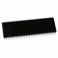
Z8018010PSG Zilog, Z8018010PSG Datasheet - Page 52

Z8018010PSG
Manufacturer Part Number
Z8018010PSG
Description
IC 10MHZ Z180 CMOS ENH MPU 64DIP
Manufacturer
Zilog
Specifications of Z8018010PSG
Processor Type
Z180
Features
8-Bit, Enhanced Z80 Megacell
Speed
10MHz
Voltage
5V
Mounting Type
Through Hole
Package / Case
64-DIP (0.750", 19.05mm)
Processor Series
Z8018xx
Core
Z80
Data Bus Width
8 bit
Maximum Clock Frequency
10 MHz
Number Of Timers
2
Operating Supply Voltage
0 V to 5 V
Maximum Operating Temperature
+ 70 C
Mounting Style
Through Hole
Minimum Operating Temperature
0 C
Core Size
8bit
Cpu Speed
10MHz
Digital Ic Case Style
DIP
No. Of Pins
64
Supply Voltage Range
4.5V To 5.5V
Operating Temperature Range
0°C To +70°C
Svhc
No SVHC (18-Jun-2010)
Base Number
8018010
Rohs Compliant
Yes
Clock Frequency
10MHz
Lead Free Status / RoHS Status
Lead free / RoHS Compliant
Other names
269-3889
Z8018010PSG
Z8018010PSG
Available stocks
Company
Part Number
Manufacturer
Quantity
Price
Company:
Part Number:
Z8018010PSG
Manufacturer:
Zilog
Quantity:
40
CSIO Control/Status Register
CSIO Control
PS014004-1106
FE: Framing Error (bit 4)—A framing error is detected when the stop bit of a character is
sampled as
becomes the oldest one in the
in the
pin is auto-enabled and is negated (High).
REI: Receive Interrupt Enable (bit 3)—
interrupt requests. When
received and
receive data from this ASCI. That is, if
IAR17–16
requests an interrupt when
DCD0
DCD0: Data Carrier Detect (bit 2 STAT0)—If bit
(
pin is High. It is cleared to
High to Low and during
auto-enabling, and the pin is negated (High), the bit 2 of
TDRE: Transmit Data Register Empty (bit 1)—
empty and the next transmit data byte is written to
TDRE
again set to
pin is auto-enabled in the
TIE: Transmit Interrupt Enable (bit 0)—
interrupt requests. If
during
CNTR: I/O Address = 0Ah—
CSIO
EF: End Flag (bit 7)—
transmit or receive operation. If the End Interrupt Enable (
CPU interrupt request is generated. Program access of
Bit
IER0
, enable and disable interrupt generation, and select the data clock speed and source.
) is
CNTLA
is cleared to
goes High.
EF
RESET
R
7
0
are
, the
0/SPACE
1
.
RDRF
10
.
register, and also by
TDRE
R/W
DCD0/CKA1
EIE
, then ASCI1 does not request an interrupt for
6
RIE
0
is set, but only if neither DMA channel sets its request-routing field to
Figure 35. CSIO Control Register
. However, this status bit is not set until or unless the error character
until the ASCI transfers the byte from
is set to
TIE = 1
is cleared to
R/W
RE
RESET
5
RIE
EF
ASEXT0
OVRN
0
, an interrupt is requested when
pin features the
is set to
on the first
1
is
RxFIFO
in
. When
1
R/W
CNTR
, the receiver requests an interrupt when a character is
TE
,
IOSTOP
4
PE
0
registers and the pin is High,
RESET
by
1
.
or
by the
FE
is used to monitor
SM1–0
IER0
RESET
READ
FE
__
, in
is cleared when software writes a
mode and during
3
is set, and ASCI0 requests an interrupt when
DCD0
is
RIE
CSIO
IOSTOP
TIE
are
.
0
of
, bit
must be set to
R/W
STAT0
must be set to
SS2
11
TDR
function, and this bit is set to
to indicate completion of an 8-bit data
2
6
and
TDRE = 1
TRDR
mode, and for ASCIO if the
of the
0
. After the byte is written to
STAT1
of the Interrupt Edge Register
SAR17–16
following the pin's transition from
CSIO
EIE
TDR
R/W
SS1
RESET
1
TDRE = 1
only occurs if
ASEXT0
RDRF
) bit =
status, enable and disable the
to the
1
indicates that the
is not used.
TDRE
1
to enable ASCI receive
to enable ASCI transmit
. On ASCIO, if the
R/W
. If
SS0
Microprocessor Unit
are
1
0
.
TSR
register is
when
TIE
RIE
is reset to
10
, or
and then
EF = 1
is cleared to
is
1
EF
1
to the
DIM1
, either ASCI
is set to
Architecture
0
1
. The
0
TDR
to select
.
when the
DCDO
TDRE
Z80180
TDR
is
EFR
CTS0
1
CSIO
is
0
and
1
,
bit
, a
is
46


