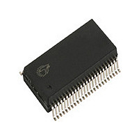
CY8C20566-24PVXIT Cypress Semiconductor Corp, CY8C20566-24PVXIT Datasheet - Page 8

CY8C20566-24PVXIT
Manufacturer Part Number
CY8C20566-24PVXIT
Description
IC MCU 32K FLASH 2K SRAM 48SSOP
Manufacturer
Cypress Semiconductor Corp
Series
CapSense® Controllersr
Specifications of CY8C20566-24PVXIT
Applications
Capacitive Sensing
Core Processor
M8C
Program Memory Type
FLASH (32 kB)
Controller Series
CY8C20xx6
Ram Size
2K x 8
Interface
I²C, SPI
Number Of I /o
36
Voltage - Supply
1.71 V ~ 5.5 V
Operating Temperature
-40°C ~ 85°C
Mounting Type
Surface Mount
Package / Case
48-SSOP
Operating Temperature (min)
-40C
Operating Temperature (max)
85C
Technology
CMOS
Processing Unit
Microprocessor
Operating Supply Voltage (min)
1.71V
Operating Supply Voltage (typ)
1.8/2.5/3.3/5V
Operating Supply Voltage (max)
5.5V
Package Type
SSOP
Screening Level
Industrial
Pin Count
48
Mounting
Surface Mount
Rad Hardened
No
Processor Series
CY8C20x66
Core
M8C
Data Bus Width
8 bit
Program Memory Size
32 KB
Data Ram Size
2 KB
Interface Type
I2C, SPI, USB
Maximum Clock Frequency
24 MHz
Number Of Programmable I/os
36
Number Of Timers
3
Maximum Operating Temperature
+ 85 C
Mounting Style
SMD/SMT
Development Tools By Supplier
CY3280-20X66
Minimum Operating Temperature
- 40 C
Lead Free Status / RoHS Status
Lead free / RoHS Compliant
Lead Free Status / RoHS Status
Compliant, Lead free / RoHS Compliant
Pinouts
The CY8C20x36/46/66/96 PSoC device is available in a variety of packages which are listed and illustrated in the following tables.
Every port pin (labeled with a “P”) is capable of Digital I/O and connection to the common analog bus. However, Vss, Vdd, and XRES
are not capable of Digital I/O.
16-Pin QFN (No E-Pad)
Table 2. Pin Definitions - CY8C20236, CY8C20246 PSoC Device
Document Number: 001-12696 Rev. *E
Notes
LEGEND A = Analog, I = Input, O = Output, OH = 5 mA High Output Drive, R = Regulated Output.
Pin
No.
1. These are the ISSP pins, which are not High Z at POR (Power On Reset).
2. During power up or reset event, device P1[1] and P1[0] may disturb the I2C bus. Use alternate pins if you encounter any issues.
10
12
13
14
15
16
11
1
2
3
4
5
6
7
8
9
Digital
IOHR
IOHR
IOHR
IOHR
IOHR
IOHR
IOHR
IOH
IOH
IOH
IOH
I/O
I/O
Power
Power
Type
Input
Analog
I
I
I
I
I
I
I
I
I
I
I
I
I
Name
XRES Active high external reset with
P2[5] Crystal output (XOut)
P2[3] Crystal input (XIn)
P1[7] I2C SCL, SPI SS
P1[5] I2C SDA, SPI MISO
P1[3] SPI CLK
P1[1] ISSP CLK
P1[0] ISSP DATA
P1[2]
P1[4] Optional external clock
P0[4]
P0[7]
P0[3] Integrating input
P0[1] Integrating input
Vdd
Vss
MOSI
Ground connection
CLK
(EXTCLK)
internal pull down
Supply voltage
Description
[1]
[1]
, I2C SCL, SPI
, I2C SDA, SPI
[2]
AI, I2C SDA, SPI MISO, P1[5]
Figure 2. CY8C20236, CY8C20246 PSoC Device
AI, I2C SCL, SPI SS, P1[7]
AI, XOut, P2[5]
AI, XIn, P2[3]
CY8C20X36/46/66/96
1
2
3
4
(Top View)
QFN
12
10
11
9
P0[4], AI
XRES
P1[2], AI
P1[4], EXTCLK, AI
Page 8 of 39
[+] Feedback


