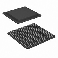
XC3S1600E-5FGG484C Xilinx Inc, XC3S1600E-5FGG484C Datasheet - Page 38

XC3S1600E-5FGG484C
Manufacturer Part Number
XC3S1600E-5FGG484C
Description
IC FPGA SPARTAN-3E 1600K 484FBGA
Manufacturer
Xilinx Inc
Series
Spartan™-3Er
Datasheet
1.XC3S100E-4VQG100C.pdf
(233 pages)
Specifications of XC3S1600E-5FGG484C
Number Of Logic Elements/cells
33192
Number Of Labs/clbs
3688
Total Ram Bits
663552
Number Of I /o
376
Number Of Gates
1600000
Voltage - Supply
1.14 V ~ 1.26 V
Mounting Type
Surface Mount
Operating Temperature
0°C ~ 85°C
Package / Case
484-BBGA
For Use With
HW-XA3S1600E-UNI-G - KIT DEVELOPMENT AUTOMOTIVE ECU
Lead Free Status / RoHS Status
Lead free / RoHS Compliant
Available stocks
Company
Part Number
Manufacturer
Quantity
Price
Company:
Part Number:
XC3S1600E-5FGG484C
Manufacturer:
XilinxInc
Quantity:
3 000
Company:
Part Number:
XC3S1600E-5FGG484C
Manufacturer:
Xilinx Inc
Quantity:
10 000
- Current page: 38 of 233
- Download datasheet (6Mb)
Functional Description
Block RAM Port Signal Definitions
Representations
RAMB16_S[w
RAMB16_S[w] with their associated signals are shown in
Figure 32a
defined in
SSR) on the block RAM are active High. However, optional
inverters on the control signals change the polarity of the
active edge to active Low.
38
Notes:
1.
2.
3.
4.
DIA[w
DIB[w
ADDRA[r
ADDRB[r
DIPB[p
DIPA[p
w
p
r
The control signals CLK, WE, EN, and SSR on both ports have the option of inverted polarity.
A
Table
A
A
and
and r
A
B
and p
and w
–p
–p
A
]_S[w
SSRA
A
A
A
SSRB
B
B
B
CLKA
CLKB
B
Figure
WEA
WEB
–1:0]
–1:0]
–1:0]
–1:0]
–1:0]
–1:0]
23. The control signals (WE, EN, CLK, and
ENA
ENB
B
B
are integers representing the address bus width at ports A and B, respectively.
are integers that indicate the number of data path lines serving as parity bits.
are integers representing the total data path width (i.e., data bits plus parity bits) at Ports A and B, respectively.
B
of
]
32b, respectively. These signals are
and
RAMB16_S
(a) Dual-Port
the
the
dual-port
W A
single-port
_S
W B
Figure 32: Block RAM Primitives
DOPA[p
DOA[w
DOPB[p
DOB[w
primitive
primitive
A
B
A
–p
B
–p
www.xilinx.com
–1:0]
–1:0]
A
B
–1:0]
–1:0]
Design Note
Whenever a block RAM port is enabled (ENA or
ENB = High), all address transitions must meet the data
sheet setup and hold times with respect to the port clock
(CLKA or CLKB), as shown in
requirement must be met even if the RAM read output is of
no interest.
ADDR[r–1:0]
DI[w–p–1:0]
DIP[p–1:0]
SSR
CLK
WE
EN
(b) Single-Port
RAMB16_Sw
DS312-2 (v3.8) August 26, 2009
Table 103, page
Product Specification
DOP[p–1:0]
DO[w–p–1:0]
DS312-2_03_111105
142.This
R
Related parts for XC3S1600E-5FGG484C
Image
Part Number
Description
Manufacturer
Datasheet
Request
R

Part Number:
Description:
IC SPARTAN-3E FPGA 1600K 320-FBG
Manufacturer:
Xilinx Inc
Datasheet:

Part Number:
Description:
IC SPARTAN-3E FPGA 1600K 400FBGA
Manufacturer:
Xilinx Inc
Datasheet:

Part Number:
Description:
IC FPGA SPARTAN-3E 1600K 320FBGA
Manufacturer:
Xilinx Inc
Datasheet:

Part Number:
Description:
IC FPGA SPARTAN-3E 1600K 320FBGA
Manufacturer:
Xilinx Inc
Datasheet:

Part Number:
Description:
IC FPGA SPARTAN-3E 1600K 400FBGA
Manufacturer:
Xilinx Inc
Datasheet:

Part Number:
Description:
IC FPGA SPARTAN 3E 320FBGA
Manufacturer:
Xilinx Inc
Datasheet:

Part Number:
Description:
IC FPGA SPARTAN 3E 400FBGA
Manufacturer:
Xilinx Inc
Datasheet:

Part Number:
Description:
IC FPGA SPARTAN 3E 484FBGA
Manufacturer:
Xilinx Inc
Datasheet:

Part Number:
Description:
FPGA, SPARTAN-3E, 1600K GATES, 484FBGA
Manufacturer:
Xilinx Inc
Datasheet:

Part Number:
Description:
PROGRAMMABLE MICROCHIP
Manufacturer:
Xilinx Inc
Datasheet:

Part Number:
Description:
FPGA Spartan®-3E Family 1.6M Gates 33192 Cells 572MHz 90nm (CMOS) Technology 1.2V 484-Pin FBGA
Manufacturer:
Xilinx Inc
Datasheet:

Part Number:
Description:
FPGA Spartan®-3E Family 1.6M Gates 33192 Cells 657MHz 90nm (CMOS) Technology 1.2V 400-Pin FBGA
Manufacturer:
Xilinx Inc
Datasheet:

Part Number:
Description:
FPGA Spartan®-3E Family 1.6M Gates 33192 Cells 657MHz 90nm (CMOS) Technology 1.2V 400-Pin FBGA
Manufacturer:
Xilinx Inc
Datasheet:

Part Number:
Description:
FPGA Spartan®-3E Family 1.6M Gates 33192 Cells 572MHz 90nm (CMOS) Technology 1.2V 320-Pin FBGA
Manufacturer:
Xilinx Inc
Datasheet:

Part Number:
Description:
IC CPLD .8K 36MCELL 44-VQFP
Manufacturer:
Xilinx Inc
Datasheet:


