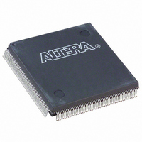
EP2C5Q208I8N Altera, EP2C5Q208I8N Datasheet - Page 54

EP2C5Q208I8N
Manufacturer Part Number
EP2C5Q208I8N
Description
IC CYCLONE II FPGA 5K 208-PQFP
Manufacturer
Altera
Series
Cyclone® IIr
Datasheet
1.EP2C5T144C8N.pdf
(168 pages)
Specifications of EP2C5Q208I8N
Number Of Logic Elements/cells
4608
Number Of Labs/clbs
288
Total Ram Bits
119808
Number Of I /o
142
Voltage - Supply
1.15 V ~ 1.25 V
Mounting Type
Surface Mount
Operating Temperature
-40°C ~ 100°C
Package / Case
208-MQFP, 208-PQFP
Family Name
Cyclone® II
Number Of Logic Blocks/elements
4608
# I/os (max)
142
Frequency (max)
402.58MHz
Process Technology
90nm
Operating Supply Voltage (typ)
1.2V
Logic Cells
4608
Ram Bits
119808
Operating Supply Voltage (min)
1.15V
Operating Supply Voltage (max)
1.25V
Operating Temp Range
-40C to 100C
Operating Temperature Classification
Industrial
Mounting
Surface Mount
Pin Count
208
Package Type
PQFP
Lead Free Status / RoHS Status
Lead free / RoHS Compliant
Number Of Gates
-
Lead Free Status / Rohs Status
Compliant
Other names
544-2135
Available stocks
Company
Part Number
Manufacturer
Quantity
Price
Company:
Part Number:
EP2C5Q208I8N
Manufacturer:
Altera
Quantity:
1 948
Company:
Part Number:
EP2C5Q208I8N
Manufacturer:
ALTERA41
Quantity:
228
Part Number:
EP2C5Q208I8N
Manufacturer:
ALTERA
Quantity:
20 000
I/O Structure & Features
Figure 2–24. Control Signal Selection per IOE
2–42
Cyclone II Device Handbook, Volume 1
Dedicated I/O
Clock [5..0]
Local
Interconnect
Local
Interconnect
Local
Interconnect
Local
Interconnect
Local
Interconnect
Local
Interconnect
io_coe
io_csclr
io_caclr
io_cce_out
io_cce_in
io_cclk
In normal bidirectional operation, you can use the input register for input
data requiring fast setup times. The input register can have its own clock
input and clock enable separate from the OE and output registers. You can
use the output register for data requiring fast clock-to-output
performance. The OE register is available for fast clock-to-output enable
timing. The OE and output register share the same clock source and the
same clock enable source from the local interconnect in the associated
LAB, dedicated I/O clocks, or the column and row interconnects. All
registers share sclr and aclr, but each register can individually disable
sclr and aclr.
configuration.
clk_in
Figure 2–25
clk_out
shows the IOE in bidirectional
ce_in
ce_out
aclr/preset
Altera Corporation
sclr/preset
February 2007
oe


