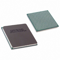
EP1S25F780C5 Altera, EP1S25F780C5 Datasheet - Page 234

EP1S25F780C5
Manufacturer Part Number
EP1S25F780C5
Description
IC STRATIX FPGA 25K LE 780-FBGA
Manufacturer
Altera
Series
Stratix®r
Datasheet
1.EP1S10F780C7.pdf
(276 pages)
Specifications of EP1S25F780C5
Number Of Logic Elements/cells
25660
Number Of Labs/clbs
2566
Total Ram Bits
1944576
Number Of I /o
597
Voltage - Supply
1.425 V ~ 1.575 V
Mounting Type
Surface Mount
Operating Temperature
0°C ~ 85°C
Package / Case
780-FBGA
Family Name
Stratix
Number Of Logic Blocks/elements
25660
# I/os (max)
597
Frequency (max)
500MHz
Process Technology
0.13um (CMOS)
Operating Supply Voltage (typ)
1.5V
Logic Cells
25660
Ram Bits
1944576
Operating Supply Voltage (min)
1.425V
Operating Supply Voltage (max)
1.575V
Operating Temp Range
0C to 85C
Operating Temperature Classification
Commercial
Mounting
Surface Mount
Pin Count
780
Package Type
FC-FBGA
Lead Free Status / RoHS Status
Contains lead / RoHS non-compliant
Number Of Gates
-
Lead Free Status / Rohs Status
Not Compliant
Other names
544-1120
Available stocks
Company
Part Number
Manufacturer
Quantity
Price
Company:
Part Number:
EP1S25F780C5
Manufacturer:
AT
Quantity:
186
Company:
Part Number:
EP1S25F780C5
Manufacturer:
ALTERA
Quantity:
315
Company:
Part Number:
EP1S25F780C5
Manufacturer:
ALTERA
Quantity:
3 000
Company:
Part Number:
EP1S25F780C5AA
Manufacturer:
ALTERA
Quantity:
269
Company:
Part Number:
EP1S25F780C5N
Manufacturer:
ALTERA
Quantity:
3 000
Timing Model
4–64
Stratix Device Handbook, Volume 1
3.3-V LVTTL
2.5-V LVTTL
1.8-V LVTTL
1.5-V LVTTL
3.3-V LVCMOS
2.5-V LVCMOS
1.8-V LVCMOS
1.5-V LVCMOS
3.3-V GTL
2.5-V GTL
3.3-V GTL+
2.5-V GTL+
3.3-V SSTL-3 Class II
3.3-V SSTL-3 Class I
2.5-V SSTL-2 Class II
2.5-V SSTL-2 Class I
1.8-V SSTL-18 Class II
1.8-V SSTL-18 Class I
1.5-V HSTL Class II
1.5-V HSTL Class I
1.8-V HSTL Class II
1.8-V HSTL Class I
3.3-V PCI
3.3-V PCI-X 1.0
3.3-V Compact PCI
3.3-V AGP 1×
Table 4–102. Reporting Methodology For Minimum Timing For Single-Ended Output Pins (Part 1 of 2)
Notes
I/O Standard
(1), (2),
(4)
(4)
(3)
(4)
(4)
–/25
–/25
–/25
–/25
R
Ω
–
–
–
–
–
–
–
–
–
–
–
–
–
–
–
–
–
–
–
–
–
–
Table 4–102
software for minimum timing information for output pins.
UP
25/–
25/–
25/–
25/–
R
Ω
–
–
–
–
–
–
–
–
–
–
–
–
–
–
–
–
–
–
–
–
–
–
DN
shows the reporting methodology used by the Quartus II
Loading and Termination
R
25
25
25
25
25
25
Ω
0
0
0
0
0
0
0
0
0
0
0
0
0
0
0
0
0
0
0
0
S
25
25
25
25
25
50
25
50
25
50
25
50
25
50
R
Ω
–
–
–
–
–
–
–
–
–
–
–
–
T
3.600
3.600
2.630
2.630
1.950
1.950
3.600
2.630
1.950
1.600
3.600
2.630
1.950
1.600
3.600
2.630
3.600
2.630
1.600
1.600
1.950
1.950
3.600
3.600
3.600
3.600
V
(V)
CCIO
3.600
2.630
1.950
1.600
3.600
2.630
1.950
1.600
1.260
1.260
1.650
1.650
1.750
1.750
1.390
1.390
1.040
1.040
0.800
0.800
0.900
0.900
1.950
1.950
3.600
3.600
VTT
(V)
(pF)
10
10
10
10
10
10
10
10
30
30
30
30
30
30
30
30
30
30
20
20
20
20
10
10
10
10
C
L
Altera Corporation
Measurement
1.026/2.214
1.026/2.214
1.026/2.214
1.026/2.214
January 2006
V
1.800
1.200
0.880
0.750
1.800
1.200
0.880
0.750
0.860
0.860
1.120
1.120
1.750
1.750
1.390
1.390
1.040
1.040
0.900
0.900
1.000
1.000
Point
MEAS


