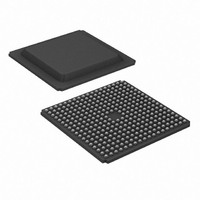
XC3S1600E-4FGG320C Xilinx Inc, XC3S1600E-4FGG320C Datasheet - Page 119

XC3S1600E-4FGG320C
Manufacturer Part Number
XC3S1600E-4FGG320C
Description
IC SPARTAN-3E FPGA 1600K 320-FBG
Manufacturer
Xilinx Inc
Series
Spartan™-3Er
Datasheet
1.XC3S100E-4VQG100C.pdf
(233 pages)
Specifications of XC3S1600E-4FGG320C
Number Of Logic Elements/cells
33192
Number Of Labs/clbs
3688
Total Ram Bits
663552
Number Of I /o
250
Number Of Gates
1600000
Voltage - Supply
1.14 V ~ 1.26 V
Mounting Type
Surface Mount
Operating Temperature
0°C ~ 85°C
Package / Case
320-BGA
For Use With
HW-XA3S1600E-UNI-G - KIT DEVELOPMENT AUTOMOTIVE ECU
Lead Free Status / RoHS Status
Lead free / RoHS Compliant
Other names
122-1481
Available stocks
Company
Part Number
Manufacturer
Quantity
Price
Company:
Part Number:
XC3S1600E-4FGG320C
Manufacturer:
XILINX
Quantity:
560
Company:
Part Number:
XC3S1600E-4FGG320C
Manufacturer:
XILINX
Quantity:
2 050
Company:
Part Number:
XC3S1600E-4FGG320C
Manufacturer:
XILINX
Quantity:
247
Part Number:
XC3S1600E-4FGG320C
Manufacturer:
XILINX/赛灵思
Quantity:
20 000
General Recommended Operating Conditions
Table 77: General Recommended Operating Conditions
DS312-3 (v3.8) August 26, 2009
Product Specification
Notes:
1.
2.
3.
4.
5.
6.
V
Symbol
V
V
V
IN
This V
range specific to each of the single-ended I/O standards, and
Each of the User I/O and Dual-Purpose pins is associated with one of the four banks’ V
internal diode junctions that exist between these pins and their associated V
is provided in
All Dedicated pins (PROG_B, DONE, TCK, TDI, TDO, and TMS) draw power from the V
that the internal diode junctions that exist between each of these pins and the V
Input voltages outside the recommended range is permissible provided that the I
exceed the range simultaneously. Refer to
See XAPP459, "Eliminating I/O Coupling Effects when Interfacing Large-Swing Single-Ended Signals to User I/O Pins."
Measured between 10% and 90% V
CCO
CCAUX
CCINT
(2,3,4,5)
T
T
IN
J
(1)
CCO
R
range spans the lowest and highest operating voltages for all supported I/O standards.
Table
Junction temperature
Internal supply voltage
Output driver supply voltage
Auxiliary supply voltage
Input voltage extremes to avoid
turning on I/O protection diodes
Input signal transition time
73.
CCO
Description
. Follow
Table
(6)
Signal Integrity
73.
Commercial
Industrial
I/O, Input-only, and
Dual-Purpose pins
Dedicated pins
www.xilinx.com
Table 82
recommendations.
lists that specific to the differential standards.
(3)
CCO
(2)
IK
and GND rails do not turn on. The absolute maximum rating
CCAUX
input clamp diode rating is met and no more than 100 pins
1.140
1.100
2.375
–0.5
–0.5
Min
–40
CCAUX
and GND rails do not turn on.
0
–
CCO
rails. Meeting the V
rail (2.5V). Meeting the V
Nominal
DC and Switching Characteristics
1.200
2.500
Table 80
–
–
–
–
–
-
lists the recommended V
V
V
CCAUX
IN
CCO
limit ensures that the
1.260
3.465
2.625
Max
100
500
85
+ 0.5
IN
+ 0.5
max limit ensures
Units
° C
° C
ns
V
V
V
V
V
CCO
119


