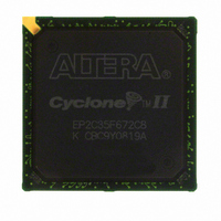
EP2C35F672C8 Altera, EP2C35F672C8 Datasheet - Page 161

EP2C35F672C8
Manufacturer Part Number
EP2C35F672C8
Description
IC CYCLONE II FPGA 33K 672-FBGA
Manufacturer
Altera
Series
Cyclone® IIr
Datasheet
1.EP2C5T144C8N.pdf
(168 pages)
Specifications of EP2C35F672C8
Number Of Logic Elements/cells
33216
Number Of Labs/clbs
2076
Total Ram Bits
483840
Number Of I /o
475
Voltage - Supply
1.15 V ~ 1.25 V
Mounting Type
Surface Mount
Operating Temperature
0°C ~ 85°C
Package / Case
672-FBGA
Family Name
Cyclone® II
Number Of Logic Blocks/elements
33216
# I/os (max)
475
Frequency (max)
402.58MHz
Process Technology
90nm
Operating Supply Voltage (typ)
1.2V
Logic Cells
33216
Ram Bits
483840
Operating Supply Voltage (min)
1.15V
Operating Supply Voltage (max)
1.25V
Operating Temp Range
0C to 85C
Operating Temperature Classification
Commercial
Mounting
Surface Mount
Pin Count
672
Package Type
FBGA
For Use With
NANO-CYCLONE - KIT NANOBOARD AND CYCLONEII DC807-1002 - DAUGHTER CARD ALTERA CYCLONE IIP0301 - DE2 CALL FOR ACADEMIC PRICING544-1733 - PCI KIT W/CYCLONE II EP2C35N
Lead Free Status / RoHS Status
Contains lead / RoHS non-compliant
Number Of Gates
-
Lead Free Status / Rohs Status
Not Compliant
Other names
544-1089
EP2C35F672C8ES
EP2C35F672C8ES
Available stocks
Company
Part Number
Manufacturer
Quantity
Price
Part Number:
EP2C35F672C8
Manufacturer:
ALTERA
Quantity:
20 000
Company:
Part Number:
EP2C35F672C8N
Manufacturer:
YAGEO
Quantity:
500 000
Company:
Part Number:
EP2C35F672C8N
Manufacturer:
ALTERA
Quantity:
500
Part Number:
EP2C35F672C8N
Manufacturer:
ALTERA/阿尔特拉
Quantity:
20 000
Altera Corporation
February 2008
Notes to
(1)
(2)
2.5-V
1.8-V
1.5-V
SSTL-2 Class I
SSTL-2 Class II
SSTL-18 Class I
SSTL-18 Class II
HSTL-18 Class I
HSTL-18 Class II
HSTL-15 Class I
HSTL-15 Class II
Differential SSTL-2 Class I
Differential SSTL-2 Class II
Differential SSTL-18 Class I
Differential SSTL-18 Class II
Differential HSTL-18 Class I
Differential HSTL-18 Class II
Differential HSTL-15 Class I
Differential HSTL-15 Class II
LVDS
Simple RSDS
Mini-LVDS
LVCMOS
LVTTL
2.5-V
1.8-V
Table 5–56. Maximum DCD for SDR Output on Column I/O
Table 5–57. Maximum for DDIO Output on Row Pins with PLL in the Clock
Path
Row Pins with PLL in the Clock Path
(Part 2 of 2)
Column I/O Output Standard
The DCD specification is characterized using the maximum drive strength
available for each I/O standard.
Numbers are applicable for commercial, industrial, and automotive devices.
Notes
Table
(1),
5–56:
(2)
(Part 1 of 2)
DC Characteristics and Timing Specifications
Cyclone II Device Handbook, Volume 1
140
115
745
150
135
150
135
C6
60
60
60
60
60
75
60
60
60
60
60
75
60
60
60
270
285
180
165
C6
140
115
745
130
135
115
150
135
130
135
115
150
135
C7
60
60
75
60
60
75
60
70
60
310
305
180
175
C7
Notes
155
165
770
130
135
115
100
150
155
130
135
115
100
150
155
C8
75
80
75
80
60
70
60
310
335
220
205
C8
(1),
(2)
Unit
Unit
ps
ps
ps
ps
ps
ps
ps
ps
ps
ps
ps
ps
ps
ps
ps
ps
ps
ps
ps
ps
ps
ps
ps
ps
ps
ps
5–71


