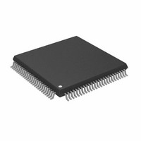
ADSP-2186BSTZ-115 Analog Devices Inc, ADSP-2186BSTZ-115 Datasheet - Page 5

ADSP-2186BSTZ-115
Manufacturer Part Number
ADSP-2186BSTZ-115
Description
IC DSP CONTROLLER 16BIT 100LQFP
Manufacturer
Analog Devices Inc
Series
ADSP-21xxr
Type
Fixed Pointr
Datasheet
1.ADSP-2186BSTZ-160.pdf
(36 pages)
Specifications of ADSP-2186BSTZ-115
Interface
Host Interface, Serial Port
Clock Rate
28.8MHz
Non-volatile Memory
External
On-chip Ram
40kB
Voltage - I/o
5.00V
Voltage - Core
5.00V
Operating Temperature
-40°C ~ 85°C
Mounting Type
Surface Mount
Package / Case
100-LQFP
Lead Free Status / RoHS Status
Lead free / RoHS Compliant
Pin Terminations (Continued)
Pin
Name
D4 or
IS
D3 or
IACK
D2:0 or
IAD15:13
PMS
DMS
BMS
IOMS
CMS
RD
WR
BR
BG
BGH
IRQ2/PF7
IRQL1/PF6
IRQL0/PF5
IRQE/PF4
SCLK0
RFS0
DR0
TFS0
DT0
SCLK1
RFS1/IRQ0
DR1/FI
TFS1/IRQ1
DT1/FO
EE
EBR
EBG
ERESET
EMS
EINT
ECLK
ELIN
ELOUT
NOTES
1. If the CLKOUT pin is not used, turn it OFF, using CLKODIS in SPORT0
2. If the Interrupt/Programmable Flag pins are not used, there are two options:
3. All bidirectional pins have three-stated outputs. When the pins are configured
4. CLKIN, RESET, and PF3:0 are not included in the table because these pins
Hi-Z = High Impedance.
autobuffer control register.
Option 1: When these pins are configured as INPUTS at reset and function as
interrupts and input flag pins, pull the pins High (inactive).
Option 2: Program the unused pins as OUTPUTS, set them to 1, and let them
float.
as an output, the output is Hi-Z (high impedance) when inactive.
must be used.
I/O
3-State
(Z)
I/O (Z)
I
I/O (Z)
I/O (Z)
I/O (Z)
O (Z)
O (Z)
O (Z)
O (Z)
O (Z)
O (Z)
O (Z)
I
O (Z)
O
I/O (Z)
I/O (Z)
I/O (Z)
I/O (Z)
I/O
I/O
I
I/O
O
I/O
I/O
I
I/O
O
I
I
O
I
O
I
I
I
O
Reset
State
Hi-Z
I
Hi-Z
Hi-Z
Hi-Z
O
O
O
O
O
O
O
I
O
O
I
I
I
I
I
I
I
O
O
I
I
I
O
O
I
I
O
I
O
I
I
I
O
Hi-Z
Caused
By
BR, EBR
BR, EBR
BR, EBR
IS
BR, EBR
BR, EBR
BR, EBR
BR, EBR
BR, EBR
BR, EBR
BR, EBR
EE
Input = High or Low,
Input = High or Low,
Unused
Configuration
Float
High (Inactive)
Float
Float
Float
Float
Float
Float
Float
Float
Float
Float
Float
High (Inactive)
Float
Float
Input = High (Inactive)
or Program as Output,
Set to 1, Let Float
Input = High (Inactive)
or Program as Output,
Set to 1, Let Float
Input = High (Inactive)
or Program as Output,
Set to 1, Let Float
Input = High (Inactive)
or Program as Output,
Set to 1, Let Float
Output = Float
High or Low
High or Low
High or Low
Float
Output = Float
High or Low
High or Low
High or Low
Float
Setting Memory Mode
Memory Mode selection for the ADSP-2186 is made during
chip reset through the use of the Mode C pin. This pin is multi-
plexed with the DSP’s PF2 pin, so care must be taken in how
the mode selection is made. The two methods for selecting the
value of Mode C are passive and active.
Passive configuration involves the use of a pull-up or pull-down
resistor connected to the Mode C pin. To minimize power
consumption, or if the PF2 pin is to be used as an output in the
DSP application, a weak pull-up or pull-down, on the order of
100 kΩ, can be used. This value should be sufficient to pull the
pin to the desired level and still allow the pin to operate as a
programmable flag output without undue strain on the processor’s
output driver. For minimum power consumption during
power-down, reconfigure PF2 to be an input, as the pull-up or
pull-down will hold the pin in a known state, and will not switch.
Active configuration involves the use of a three-stateable exter-
nal driver connected to the Mode C pin. A driver’s output en-
able should be connected to the DSP’s RESET signal such that
it only drives the PF2 pin when RESET is active (low). After
RESET is deasserted, the driver should three-state, thus allow-
ing full use of the PF2 pin as either an input or output.
To minimize power consumption during power-down, configure
the programmable flag as an output when connected to a three-
stated buffer. This ensures that the pin will be held at a constant
level and not oscillate should the three-state driver’s level hover
around the logic switching point.
Interrupts
The interrupt controller allows the processor to respond to the
eleven possible interrupts and reset with minimum overhead.
The ADSP-2186 provides four dedicated external interrupt
input pins, IRQ2, IRQL0, IRQL1 and IRQE (shared with the
PF7:4 pins). In addition, SPORT1 may be reconfigured for
IRQ0, IRQ1, FI and FO, for a total of six external interrupts.
The ADSP-2186 also supports internal interrupts from the
timer, the byte DMA port, the two serial ports, software and the
power-down control circuit. The interrupt levels are internally
prioritized and individually maskable (except power-down and
RESET). The IRQ2, IRQ0 and IRQ1 input pins can be pro-
grammed to be either level- or edge-sensitive. IRQL0 and IRQL1
are level-sensitive and IRQE is edge-sensitive. The priorities and
vector addresses of all interrupts are shown in Table I.
Source Of Interrupt
Reset (or Power-Up with
Power-Down (Nonmaskable) 002C
IRQ2
IRQL1
IRQL0
SPORT0 Transmit
SPORT0 Receive
IRQE
BDMA Interrupt
SPORT1 Transmit or IRQ1 0020
SPORT1 Receive or IRQ0
Timer
Table I. Interrupt Priority and Interrupt Vector Addresses
PUCR = 1)
Interrupt Vector Address (Hex)
0000 (Highest Priority)
0004
0008
000C
0010
0014
0018
001C
0024
0028 (Lowest Priority)
ADSP-2186


