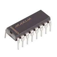
MAX500ACPE Maxim Integrated Products, MAX500ACPE Datasheet - Page 10

MAX500ACPE
Manufacturer Part Number
MAX500ACPE
Description
IC DAC QUAD SERIAL-INTER 16-DIP
Manufacturer
Maxim Integrated Products
Datasheet
1.MAX500BCPE.pdf
(12 pages)
Specifications of MAX500ACPE
Settling Time
2.5µs
Number Of Bits
8
Data Interface
Serial
Number Of Converters
4
Voltage Supply Source
Dual ±
Operating Temperature
0°C ~ 70°C
Mounting Type
Through Hole
Package / Case
16-DIP (0.300", 7.62mm)
Lead Free Status / RoHS Status
Contains lead / RoHS non-compliant
Power Dissipation (max)
-
Available stocks
Company
Part Number
Manufacturer
Quantity
Price
Company:
Part Number:
MAX500ACPE
Manufacturer:
MAXIM
Quantity:
5 510
Careful PC board ground layout techniques should be
used to minimize crosstalk between DAC outputs, the
reference input(s), and the digital inputs. This is partic-
ularly important if the reference is driven from an AC
source. Figure 7 shows suggested PC board layouts for
minimizing crosstalk.
In unipolar operation, the output voltages and the refer-
ence input(s) are the same polarity. The unipolar circuit
configuration is shown in Figure 8 for the MAX500. The
device can be operated from a single supply with a
slight increase in zero error (see Output Buffer
Amplifiers section). To avoid parasitic device turn-on,
the voltage at V
respect to AGND. The unipolar code table is given in
Table 3.
Each DAC output may be configured for bipolar opera-
tion using the circuit in Figure 9. One op amp and two
resistors are required per channel. With R1 = R2:
where D
word in Register A.
Table 4 shows the digital code versus output voltage
for the circuit in Figure 9.
CMOS, Quad, Serial-Interface
8-Bit DAC
Table 3. Unipolar Code Table
Note: 1LSB = (V
10
1 1 1 1
1 0 0 0
1 0 0 0
0 1 1 1
0 0 0 0
0 0 0 0
______________________________________________________________________________________
MSB
DAC CONTENTS
A
is a fractional representation of the digital
REF
V
) (2
OUT
REF
1 1 1 1
0 0 0 1
0 0 0 0
1 1 1 1
0 0 0 1
0 0 0 0
-8
LSB
) = +V
= V
must always be positive with
REF
REF
(2D
(
256
–––
+V
1
A
Unipolar Output
REF
)
- 1)
+V
+V
+V
+V
Bipolar Output
ANALOG
OUTPUT
(
REF
REF
REF
REF
––––
128
256
0V
(
(
(
(
––––
––––
––––
––––
)
255
256
129
256
256
256
127
1
= +
)
)
)
)
V
––––
REF
2
AGND can be biased above DGND to provide an arbi-
trary nonzero output voltage for a “zero” input code. This
is shown in Figure 10. The output voltage at V
where D
input word. Since AGND is common to all four DACs,
all outputs will be offset by V
Since AGND current is a function of the four DAC
codes, it should be driven by a low-impedance source.
V
Table 4. Bipolar Code Table
Note: 1LSB = (V
Figure 10. AGND Bias Circuit
BIAS
V
V
BIAS
+
+
-
-
IN
1 1 1 1
1 0 0 0
1 0 0 0
0 1 1 1
0 0 0 0
0 0 0 0
DIGITAL INPUTS NOT SHOWN
MSB
must be positive.
DAC CONTENTS
A
V
is a fractional representation of the digital
OUT
5
AGND
REF
A = V
-5V (OR GND)
) (2
DAC A
V
1 1 1 1
0 0 0 1
0 0 0 0
1 1 1 1
0 0 0 1
0 0 0 0
SS
-8
LSB
BIAS
4
V
3
REF
) = +V
A/B
+ D
MAX500
REF
BIAS
A
V
(
IN
256
–––
DGND
+15V
1
V
Offsetting AGND
DD
in the same manner.
-V
6
14
)
REF
+V
+V
-V
-V
ANALOG
OUTPUT
REF
REF
REF
REF
(
––––
128
128
0V
(
(
(
(
OUT
––––
––––
127
––––
128
––––
128
127
128
128
1
)
1
= -V
2
A is:
)
)
)
)
REF
V
OUT
A


