MAX512CPD Maxim Integrated Products, MAX512CPD Datasheet - Page 8
MAX512CPD
Manufacturer Part Number
MAX512CPD
Description
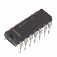
IC DAC TRPL VOLT-OUT 8BIT 14-DIP
Manufacturer
Maxim Integrated Products
Datasheet
1.MAX512CPD.pdf
(16 pages)
Specifications of MAX512CPD
Settling Time
70µs
Number Of Bits
8
Data Interface
Serial
Number Of Converters
3
Voltage Supply Source
Dual ±
Operating Temperature
0°C ~ 70°C
Mounting Type
Through Hole
Package / Case
14-DIP (0.300", 7.62mm)
Lead Free Status / RoHS Status
Contains lead / RoHS non-compliant
Power Dissipation (max)
-
Available stocks
Company
Part Number
Manufacturer
Quantity
Price

Part Number:
MAX512CPD
Manufacturer:
MAXIM/美信
Quantity:
20 000


Low-Cost, Triple, 8-Bit Voltage-Output DACs
with Serial Interface
(T
8
_____________________________Typical Operating Characteristics (continued)
______________________________________________________________Pin Description
A
PIN
10
11
12
13
14
1
2
3
4
5
6
7
8
9
= +25°C, unless otherwise noted.)
_______________________________________________________________________________________
A: CS, 2V/div
B: OUTA, 1V/div
V
DAC LOADED WITH ALL 1s
DD
–
R
REFAB
—
NAME
OUTA
OUTB
OUTC
SCLK
REFC
LOUT
= 3V, V
GND
E
V
DIN
—
V
I.C.
–
C
—
S
DD
SS
—
S
–
TIME EXITING SHUTDOWN MODE
E
—
SS
T
–
= 0V, REFAB = V
Serial Data Input of the 16-bit shift register. Data is clocked into the register on the rising edge of SCLK.
Chip Select (active low). Enables data to be shifted into the 16-bit shift register. Programming commands
are executed at the rising edge of
Serial Clock Input. Data is clocked in on the rising edge of SCLK.
Asynchronous reset input (active low). Clears all registers to their default state (FFhex for DAC A and
DAC B registers); all other registers are reset to 0 (including the input shift register).
Positive Power Supply (2.7V to 5.5V). Bypass with 0.22µF to GND.
Ground
Negative Power Supply 0V or (-1.5V to -5.5V). Tie to GND for single supply operation. If a negative supply
is applied, bypass with 0.22µF to GND.
DAC A Output Voltage (Buffered). Resets to full scale. Connect 0.1µF capacitor or greater to GND.
DAC B Output Voltage (Buffered). Resets to full scale. Connect 0.01µF capacitor or greater to GND.
DAC C Output Voltage (Unbuffered). Resets to zero.
DAC C Reference Voltage
DAC A/B Reference Voltage
Internally connected. Do not make connections to this pin.
Logic Output (latched)
20 s/div
DD,
R
L
= 1k , C
L
= 0.1 F
A
B
–
C
—
S
–
.
FUNCTION
DIGITAL CODE = 80, REFAB = V
OUTPUT VOLTAGE NOISE DC TO 1MHz
2ms/div
DD,
NO LOAD
OUTA,
200 V/div
Related parts for MAX512CPD
Image
Part Number
Description
Manufacturer
Datasheet
Request
R

Part Number:
Description:
MAX7528KCWPMaxim Integrated Products [CMOS Dual 8-Bit Buffered Multiplying DACs]
Manufacturer:
Maxim Integrated Products
Datasheet:
Part Number:
Description:
Single +5V, fully integrated, 1.25Gbps laser diode driver.
Manufacturer:
Maxim Integrated Products
Datasheet:
Part Number:
Description:
Single +5V, fully integrated, 155Mbps laser diode driver.
Manufacturer:
Maxim Integrated Products
Datasheet:
Part Number:
Description:
VRD11/VRD10, K8 Rev F 2/3/4-Phase PWM Controllers with Integrated Dual MOSFET Drivers
Manufacturer:
Maxim Integrated Products
Datasheet:
Part Number:
Description:
Highly Integrated Level 2 SMBus Battery Chargers
Manufacturer:
Maxim Integrated Products
Datasheet:
Part Number:
Description:
Current Monitor and Accumulator with Integrated Sense Resistor; ; Temperature Range: -40°C to +85°C
Manufacturer:
Maxim Integrated Products
Part Number:
Description:
TSSOP 14/A�/RS-485 Transceivers with Integrated 100O/120O Termination Resis
Manufacturer:
Maxim Integrated Products
Part Number:
Description:
TSSOP 14/A�/RS-485 Transceivers with Integrated 100O/120O Termination Resis
Manufacturer:
Maxim Integrated Products
Part Number:
Description:
QFN 16/A�/AC-DC and DC-DC Peak-Current-Mode Converters with Integrated Step
Manufacturer:
Maxim Integrated Products
Part Number:
Description:
TDFN/A/65V, 1A, 600KHZ, SYNCHRONOUS STEP-DOWN REGULATOR WITH INTEGRATED SWI
Manufacturer:
Maxim Integrated Products
Part Number:
Description:
Integrated Temperature Controller f
Manufacturer:
Maxim Integrated Products
Part Number:
Description:
SOT23-6/I�/45MHz to 650MHz, Integrated IF VCOs with Differential Output
Manufacturer:
Maxim Integrated Products
Part Number:
Description:
SOT23-6/I�/45MHz to 650MHz, Integrated IF VCOs with Differential Output
Manufacturer:
Maxim Integrated Products
Part Number:
Description:
EVALUATION KIT/2.4GHZ TO 2.5GHZ 802.11G/B RF TRANSCEIVER WITH INTEGRATED PA
Manufacturer:
Maxim Integrated Products
Part Number:
Description:
QFN/E/DUAL PCIE/SATA HIGH SPEED SWITCH WITH INTEGRATED BIAS RESISTOR
Manufacturer:
Maxim Integrated Products
Datasheet: