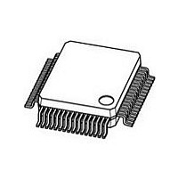
SC16C554BIBM NXP Semiconductors, SC16C554BIBM Datasheet - Page 30

SC16C554BIBM
Manufacturer Part Number
SC16C554BIBM
Description
Manufacturer
NXP Semiconductors
Datasheet
1.SC16C554BIBM.pdf
(58 pages)
Specifications of SC16C554BIBM
Transmit Fifo
16Byte
Receive Fifo
16Byte
Transmitter And Receiver Fifo Counter
Yes
Data Rate
5Mbps
Package Type
LQFP
Operating Supply Voltage (max)
5.5V
Mounting
Surface Mount
Operating Temperature (min)
-40C
Operating Temperature (max)
85C
Operating Temperature Classification
Industrial
Lead Free Status / Rohs Status
Compliant
Available stocks
Company
Part Number
Manufacturer
Quantity
Price
Company:
Part Number:
SC16C554BIBM
Manufacturer:
NXP
Quantity:
673
Company:
Part Number:
SC16C554BIBM,151
Manufacturer:
NXP Semiconductors
Quantity:
10 000
Company:
Part Number:
SC16C554BIBM-S
Manufacturer:
TDK
Quantity:
4 000
NXP Semiconductors
SC16C554B_554DB
Product data sheet
7.3.2 FIFO mode
Table 11.
Bit
7:6
5:4
3
2
1
0
Symbol
FCR[7:6]
FCR[5:4]
FCR[3]
FCR[2]
FCR[1]
FCR[0]
FIFO Control Register bits description
All information provided in this document is subject to legal disclaimers.
5 V, 3.3 V and 2.5 V quad UART, 5 Mbit/s (max.) with 16-byte FIFOs
Description
RCVR trigger. These bits are used to set the trigger level for the receive
FIFO interrupt.
An interrupt is generated when the number of characters in the FIFO equals
the programmed trigger level. However, the FIFO will continue to be loaded
until it is full. Refer to
not used; initialized to logic 0
DMA mode select.
Transmit operation in mode ‘0’: When the SC16C554B/554DB is in the
16C450 mode (FIFOs disabled; FCR[0] = logic 0) or in the FIFO mode
(FIFOs enabled; FCR[0] = logic 1; FCR[3] = logic 0), and when there are no
characters in the transmit FIFO or Transmit Holding Register, the TXRDY
pin will be a logic 0. Once active, the TXRDY pin will go to a logic 1 after the
first character is loaded into the Transmit Holding Register.
Receive operation in mode ‘0’: When the SC16C554B/554DB is in
mode ‘0’ (FCR[0] = logic 0), or in the FIFO mode (FCR[0] = logic 1;
FCR[3] = logic 0) and there is at least one character in the receive FIFO, the
RXRDY pin will be a logic 0. Once active, the RXRDY pin will go to a logic 1
when there are no more characters in the receiver.
Transmit operation in mode ‘1’: When the SC16C554B/554DB is in FIFO
mode (FCR[0] = logic 1; FCR[3] = logic 1), the TXRDY pin will be a logic 1
when the transmit FIFO is completely full. It will be a logic 0 if one or more
FIFO locations are empty.
Receive operation in mode ‘1’: When the SC16C554B/554DB is in FIFO
mode (FCR[0] = logic 1; FCR[3] = logic 1) and the trigger level has been
reached, or a Receive Time-out has occurred, the RXRDY pin will go to a
logic 0. Once activated, it will go to a logic 1 after there are no more
characters in the FIFO.
XMIT FIFO reset.
RCVR FIFO reset.
FIFO enable.
logic 0 = set DMA mode ‘0’ (normal default condition)
logic 1 = set DMA mode ‘1’
logic 0 = no FIFO transmit reset (normal default condition)
logic 1 = clears the contents of the transmit FIFO and resets the FIFO
counter logic (the Transmit Shift Register is not cleared or altered). This
bit will return to a logic 0 after clearing the FIFO.
logic 0 = no FIFO receive reset (normal default condition)
logic 1 = clears the contents of the receive FIFO and resets the FIFO
counter logic (the Receive Shift Register is not cleared or altered). This bit
will return to a logic 0 after clearing the FIFO.
logic 0 = disable the transmit and receive FIFO (normal default condition)
logic 1 = enable the transmit and receive FIFO. This bit must be a 1
when other FCR bits are written to, or they will not be programmed.
Rev. 4 — 8 June 2010
Table
12.
SC16C554B/554DB
© NXP B.V. 2010. All rights reserved.
30 of 58


