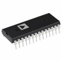
AD667KN Analog Devices Inc, AD667KN Datasheet - Page 3

AD667KN
Manufacturer Part Number
AD667KN
Description
IC DAC 12BIT W/BUFF LATCH 28-DIP
Manufacturer
Analog Devices Inc
Datasheet
1.AD667JNZ.pdf
(8 pages)
Specifications of AD667KN
Mounting Type
Through Hole
Rohs Status
RoHS non-compliant
Settling Time
3µs
Number Of Bits
12
Number Of Converters
1
Voltage Supply Source
Dual ±
Power Dissipation (max)
1W
Operating Temperature
0°C ~ 70°C
Package / Case
28-DIP (0.600", 15.24mm)
Resolution (bits)
12bit
No. Of Pins
28
Peak Reflow Compatible (260 C)
No
Update Rate
0.5MSPS
No. Of Bits
12 Bit
Leaded Process Compatible
No
Interface Type
Serial
Data Interface
-
Lead Free Status / RoHS Status
Contains lead / RoHS non-compliant
Available stocks
Company
Part Number
Manufacturer
Quantity
Price
Company:
Part Number:
AD667KN
Manufacturer:
MAXIM
Quantity:
5 510
Part Number:
AD667KN
Manufacturer:
ADI/亚德诺
Quantity:
20 000
Model
DIGITAL INPUTS
TRANSFER CHARACTERISTICS
DRIFT
CONVERSION SPEED
ANALOG OUTPUT
REFERENCE OUTPUT
POWER SUPPLY SENSITIVITY
POWER SUPPLY REQUIREMENTS
TEMPERATURE RANGE
TIMING DIAGRAMS
WRITE CYCLE #1
(Load First Rank from Data Bus; A3 = 1)
REV. A
Resolution
Logic Levels (TTL, Compatible, T
V
V
I
I
ACCURACY
Differential Linearity
Gain (Full Scale) T
Unipolar Offset T
Bipolar Zero T
Settling Time to 0.01% of FSR for
Ranges
Output Current
Output Impedance (DC)
Short Circuit Current
External Current
V
V
Rated Voltages
Range
Supply Current
Specification
Storage
IH
IL
IH
IL
CC
EE
Linearity Error @ +25 C
Differential Linearity Error @ +25 C
Gain Error
Unipolar Offset Error
Bipolar Zero
FSR Change (2 k
For LSB Change
+11.4 V to +16.5 V dc
–11.4 V to –16.5 V dc
(V
(V
(Logic “0”)
(Logic “l’’)
= –11.4 V to –16.5 V dc
= +11.4 V to +16.5 V dc
T
T
with 10 k Feedback
with 5 k Feedback
Slew Rate
IL
IH
4
A
A
4
= 0.8 V)
= 5.5 V)
= T
= T
MIN
MIN
2
A
2
to T
to T
= 25 C to T
A
A
= 25 C to T
= 25 C to T
MAX
MAX
500 pF Load)
2
MIN
MIN
MIN
MIN
or T
or T
or T
–T
MAX
MAX
MAX
MAX
)
1
Min
+2.0
0
Monotonicity Guaranteed
10
9.90
0.1
–25
–65
5
11.4
AD667A
Typ
3
1
+1/4
3
2
1
+5, +10
0.05
10.00
1.0
5
5
8
20
1/2
1/2
0.1
1
0.05
2
5
1
5
2.5, 5, 10,
12, 15
Max
+5.5
+0.8
10
5
4
3
10.10
10
10
12
25
+85
+150
12
40
30
3
10
1/2
3/4
3/4
0.2
2
0.1
16.5
–3–
Min
+2.0
0
Monotonicity Guaranteed
10
9.90
0.1
–25
–65
5
11.4
WRITE CYCLE #2
(Load Second Rank from First Rank; A2, A1, A0 = 1)
AD667B
3
3
2
1
+5, +10
5
Typ
1
0.05
10.00
1.0
5
8
20
1/8
1/4
1/4
0.1
1
0.05
2
5
2.5, 5, 10,
12, 15
Max
+5.5
+0.8
10
5
4
3
10.10
10
10
12
25
+85
+150
12
40
15
3
10
1/4
1/2
1/2
0.2
2
0.1
16.5
Min
+2.0
0
Monotonicity Guaranteed
10
9.90
1.0
–55
–65
5
11.4
AD667S
Typ
3
1
3
2
1
+5, +10
0.05
10.00
5
5
8
20
1/8
1/8
1/4
0.1
1
0.05
2
15
2.5, 5, 10,
12, 15
Max
12
+5.5
+0.7
10
5
4
3
40
10.10
10
10
12
25
+125
+150
1/2
3/4
3/4
0.2
2
0.1
30
3
10
16.5
Units
Bits
V
V
LSB
LSB
LSB
LSB
% FSR
LSB
% of FSR
ppm of FSR/ C
ppm of FSR/ C
ppm of FSR/ C
ppm of FSR/ C
V/ s
V
mA
mA
V
mA
ppm of FS/%
ppm of FS/%
V
V
mA
mA
C
C
A
A
s
s
s
AD667
3


