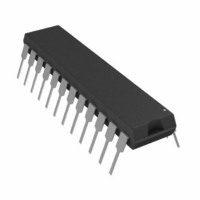
AD7537KNZ Analog Devices Inc, AD7537KNZ Datasheet - Page 4

AD7537KNZ
Manufacturer Part Number
AD7537KNZ
Description
IC DAC 12BIT DUAL MULT 24DIP
Manufacturer
Analog Devices Inc
Datasheet
1.AD7537JNZ.pdf
(8 pages)
Specifications of AD7537KNZ
Data Interface
Parallel
Settling Time
250µs
Number Of Bits
12
Number Of Converters
2
Voltage Supply Source
Single Supply
Power Dissipation (max)
24mW
Operating Temperature
-40°C ~ 85°C
Mounting Type
Through Hole
Package / Case
24-DIP (0.300", 7.62mm)
Resolution (bits)
12bit
Sampling Rate
667kSPS
Input Channel Type
Parallel
Supply Current
2mA
Digital Ic Case Style
DIP
No. Of Pins
24
Number Of Channels
2
Resolution
12b
Conversion Rate
667KSPS
Interface Type
Parallel
Single Supply Voltage (typ)
12/15V
Dual Supply Voltage (typ)
Not RequiredV
Architecture
R-2R
Power Supply Requirement
Single
Output Type
Current
Integral Nonlinearity Error
±0.5LSB
Single Supply Voltage (min)
10.8V
Single Supply Voltage (max)
16.5V
Dual Supply Voltage (min)
Not RequiredV
Dual Supply Voltage (max)
Not RequiredV
Operating Temp Range
-40C to 85C
Operating Temperature Classification
Industrial
Mounting
Through Hole
Pin Count
24
Package Type
PDIP
Lead Free Status / RoHS Status
Lead free / RoHS Compliant
Lead Free Status / RoHS Status
Lead free / RoHS Compliant, Lead free / RoHS Compliant
Available stocks
Company
Part Number
Manufacturer
Quantity
Price
AD7537
PIN
1
2
3
4
5
6–14
12
15
16
17
18
19
20
21
22
23
24
CIRCUIT INFORMATION – D/A SECTION
The AD7537 contains two identical 12-bit multiplying D/A
converters. Each DAC consists of a highly stable R-2R ladder
and 12 N-channel current steering switches. Figure 2 shows a
simplified D/A circuit for DAC A. In the R-2R ladder, binary
weighted currents are steered between I
MNEMONIC
AGNDA
I
R
V
CS
DB0–DB7
DGND
A0
A1
CLR
WR
UPD
V
V
R
I
AGNDB
OUTA
OUTB
FBA
REFA
DD
REFB
FBB
PIN FUNCTION DESCRIPTION (DIP)
DIP
PIN CONFIGURATIONS
DESCRIPTION
Analog Ground for DAC A.
Current output terminal of DAC A.
Feedback resistor for DAC A.
Reference input to DAC A.
Chip Select Input Active low.
Eight data inputs, DB0–DB7.
Digital Ground.
Address Line 0.
Address Line 1.
Clear Input. Active low. Clears all
registers.
Write Input. Active low.
Updates DAC Registers from inputs
registers.
Power supply input. Nominally +12 V
to +15 V, with 10% tolerance.
Reference input to DAC B.
Feedback resistor for DAC B.
Current output terminal of DAC B.
Analog Ground for DAC B.
PLCC
OUTA
LCCC
and AGNDA. The
–4–
current flowing in each ladder leg is constant, irrespective of
switch state. The feedback resistor R
(see Figures 4 and 5) to convert the current flowing in I
a voltage output.
EQUIVALENT CIRCUIT ANALYSIS
Figure 3 shows the equivalent circuit for one of the D/A con-
verters (DAC A) in the AD7537. A similar equivalent circuit
can be drawn for DAC B.
C
and varies from about 50 pF to 150 pF with digital input code.
The current source I
leakages and approximately doubles every 10 C. R
equivalent output resistance of the device which varies with
input code.
DIGITAL CIRCUIT INFORMATION
The digital inputs are designed to be both TTL and 5 V CMOS
compatible. All logic inputs are static protected MOS gates with
typical input currents of less than 1 nA.
CLR UPD CS WR A1 A0 FUNCTION
1
1
0
1
1
1
1
1
1
NOTES: X = Don’t care
OUT
is the output capacitance due to the N-channel switches
Figure 2. Simplified Circuit Diagram for DAC A
1
1
X
1
1
1
1
0
0
Figure 3. Equivalent Analog Circuit for DAC A
1
X
X
0
0
0
0
1
0
Table I. AD7537 Truth Table
X
1
X
0
0
0
0
0
0
LKG
X
X
X
0
0
1
1
X
X
is composed of surface and junction
X
X
X
0
1
0
1
X
X
No Data Transfer
No Data Transfer
All Registers Cleared
DAC A LS Input Register
Loaded with DB7–DB0 (LSB)
DAC A MS Input Register
Loaded with DB3 (MSB)–DB0
DAC B LS Input Register
Loaded with DB7–DB0 (LSB)
DAC B MS Input Register
Loaded with DB3 (MSB)–DB0
DAC A, DAC B Registers
Updated Simultaneously from
Input Registers
DAC A, DAC B Registers are
Transparent
FBA
is used with an op amp
0
is the
OUTA
REV. 0
to


