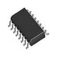
SI4720CY-T1 Vishay, SI4720CY-T1 Datasheet - Page 2

SI4720CY-T1
Manufacturer Part Number
SI4720CY-T1
Description
Manufacturer
Vishay
Datasheet
1.SI4720CY-T1.pdf
(9 pages)
Specifications of SI4720CY-T1
Power Switch Family
Si4720CY
Input Voltage
0 to 13.2V
Power Switch On Resistance
15.5mOhm
Output Current
0A
Number Of Outputs
Dual
Mounting
Surface Mount
Supply Current
1.1uA
Package Type
SOIC N
Operating Temperature (min)
-25C
Operating Temperature (max)
85C
Operating Temperature Classification
Commercial
Pin Count
16
Power Dissipation
2.5W
Lead Free Status / Rohs Status
Not Compliant
Available stocks
Company
Part Number
Manufacturer
Quantity
Price
Company:
Part Number:
SI4720CY-T1-E3
Manufacturer:
Freescale
Quantity:
41
Voltage Referenced to GND
V
V
V
V
Stresses beyond those listed under “Absolute Maximum Ratings” may cause permanent damage to the device. These are stress ratings only, and functional operation
of the device at these or any other conditions beyond those indicated in the operational sections of the specifications is not implied. Exposure to absolute maximum rating
conditions for extended periods may affect device reliability.
V
V
I
Notes
a.
b.
c.
d.
www.vishay.com FaxBack 408-970-5600
2-2
Si4720CY
Vishay Siliconix
DS
On-Resistance
Leakage Current
Supply Current
Supply Current
Input Voltage Low
Input Voltage High
Input Leakage Current
Turn-On Delay
Turn-Off Delay
Break-Before-Make
Rise Time
Fall Time
Voltage Across Pin 6 and 7
Forward Diode
S
SD
IN1
GS
S
IN1
, V
, V
Room = 25 C, Full = as determined by the operating temperature suffix.
The algebraic convention whereby the most negative value is a minimum and the most positive a maximum.
Typical values are for DESIGN AID ONLY, not guaranteed nor subject to production testing.
Guaranteed by design, not subject to production testing.
, V
, V
. . . . . . . . . . . . . . . . . . . . . . . . . . . . . . . . . . . . . .
D
D
. . . . . . . . . . . . . . . . . . . . . . . . . . . . . . . . . .
. . . . . . . . . . . . . . . . . . . . . . . . . . . . . . . . . . . . . . . . . .
a
P
Parameter
IN2
IN2
. . . . . . . . . . . . . . . . . . . . . . . . . . . . . . . . . .
. . . . . . . . . . . . . . . . . . . . . . . . . . . . . . .
. . . . . . . . . . . . . . . . . . . . . . . . . . . . .
. . . . . . . . . . . . . . . . . . . . . . . . . . . . . .
d
t D
to D or S
IN
S
S
Symbol
t
I
t
OFF(IN)
DS(off)
I
I
ON(IN)
t
t
V
t
V
V
V
S(off)
S(on)
I
RISE
FALL
r
BBM
INH
DS
INH
INL
GS
SD
b l
Unless Otherwise Specified
–0.3 V to 32 V
–0.3 V to 30 V
–0.3 V to 15 V
V
V
V
V
0 V to 13.2 V
V
S
S
S
S
V
V
S
6 V to 30 V
= 10 V, R
= 10 V, R
= 10 V, R
= 10 V, R
Test Conditions
Test Conditions
S
S
= 10 V, I
0 A to 6 A
= 10 V and V
= 10 V and V
V
V
V
V
V
I
DS
IN
D
20 V
S
S
S
D
L
L
L
L
= –1 A
= 21 V
= 21 V
= 5.0 V
= 30 V
= 10 V
= 5
= 5
= 5
= 5
= 1 A, V
S
S
, Figure 1
, Figure 1
, Figure 1
, Figure 1
= 21 V
= 21 V
IN
= H
Storage Temperature
Power Dissipation
Notes
a.
b.
Operating Temperature Range
Junction Temperature
V
Device mounted with all leads soldered to 1” x 1” FR4 with laminated
copper PC board.
SD
30 V
Temp
Room
Room
Room
Room
Room
Room
Room
Room
Room
Room
Room
DC
Full
Full
Full
a
b
Min
(t = 10 sec)
(t = steady state)
2.5
2.2
. . . . . . . . . . . . . . . . . . .
. . . . . . . . . . . . . . . . . . .
b
Limits
0.0155
Typ
1.05
10.2
1.1
2.9
1.5
1.3
50
. . . . . . . . . . . .
c
. . . . . . . . . . . . . . . .
S-49524—Rev. B, 21-Jul-97
Document Number: 70664
. . . . . . . . . . .
Max
0.020
100
2.1
2.5
1.1
10
18
1
1
6
1
5
–55 to 150 C
–25 to 150 C
b
–25 to 85 C
2.5 W
1.5 W
Unit
ns
V
V
V
V
A
A
A
s
s


