AD5582YRVZ Analog Devices Inc, AD5582YRVZ Datasheet

IC DAC 12BIT QUAD VOUT 48-TSSOP

AD5582YRVZ

Manufacturer Part Number
AD5582YRVZ
Description
IC DAC 12BIT QUAD VOUT 48-TSSOP
Manufacturer
Analog Devices Inc
Datasheet

Specifications of AD5582YRVZ

Data Interface
Parallel
Settling Time
5µs
Number Of Bits
12
Number Of Converters
4
Voltage Supply Source
Analog and Digital, Dual ±
Power Dissipation (max)
30mW
Operating Temperature
-40°C ~ 125°C
Mounting Type
Surface Mount
Package / Case
48-TSSOP
Resolution (bits)
12bit
Sampling Rate
200kSPS
Input Channel Type
Parallel
Supply Current
2.3mA
Digital Ic Case Style
TSSOP
No. Of Pins
48
Number Of Channels
4
Resolution
12b
Conversion Rate
200KSPS
Interface Type
Parallel
Single Supply Voltage (typ)
5/15V
Dual Supply Voltage (typ)
±5V
Architecture
R-2R
Power Supply Requirement
Single/Dual
Output Type
Voltage
Integral Nonlinearity Error
±1LSB
Single Supply Voltage (min)
3V
Single Supply Voltage (max)
18V
Dual Supply Voltage (min)
±2.7V
Dual Supply Voltage (max)
±6.5V
Operating Temp Range
-40C to 125C
Operating Temperature Classification
Automotive
Mounting
Surface Mount
Pin Count
48
Package Type
TSSOP
Lead Free Status / RoHS Status
Lead free / RoHS Compliant
Lead Free Status / RoHS Status
Lead free / RoHS Compliant, Lead free / RoHS Compliant

Available stocks

Company
Part Number
Manufacturer
Quantity
Price
Part Number:
AD5582YRVZ
Manufacturer:
ADI/亚德诺
Quantity:
20 000
a
GENERAL DESCRIPTION
The AD5582/AD5583 family of quad, 12-/10-bit, voltage output
digital-to-analog converters is designed to operate from a single
5 V to 15 V or dual ±5 V supply. It offers the user ease of use in
single- or dual-supply systems. Built using an advance BiCMOS
process, this high performance DAC is dynamically stable, capable
of high current drive, and in small form factor.
The applied external reference V
put voltage ranges from V
of full-scale outputs. For multiplying and wide dynamic appli-
cations, ac reference inputs can be as high as |V
built-in precision trimmed resistors are available and can be
configured easily to provide four-quadrant multiplications.
A doubled-buffered parallel interface offers a fast settling time.
A common level sensitive load DAC strobe (LDAC) input allows
additional simultaneous update of all DAC outputs. An external
asynchronous reset (RS) forces all registers to the zero code state
when the MSB = 0 or to midscale when the MSB = 1.
Both parts are offered in the same pinout and package to allow
users to select the appropriate resolution for a given application
without PCB layout changes.
REV. A
Information furnished by Analog Devices is believed to be accurate and
reliable. However, no responsibility is assumed by Analog Devices for its
use, nor for any infringements of patents or other rights of third parties that
may result from its use. No license is granted by implication or otherwise
under any patent or patent rights of Analog Devices. Trademarks and
registered trademarks are the property of their respective companies.
FEATURES
12-Bit Linearity and Monotonic AD5582
10-Bit Linearity and Monotonic AD5583
Wide Operating Range: Single 5 V to 15 V or
Unipolar or Bipolar Operation
Double Buffered Registers Enable Independent or
4 Independent Rail-to-Rail Reference Inputs
20 mA High Current Output Drive
Parallel Interface
Data Readback Capability
5 s Settling Time
Built-In Matching Resistor Simplifies
Unconditionally Stable Under Any Capacitive Loading
Compact Footprint: TSSOP-48
Extended Temperature Range:
APPLICATIONS
Process Control Equipment
Closed-Loop Servo Control
Data Acquisition Systems
Digitally Controlled Calibration
Optical Network Control Loops
4 m to 20 mA Current Transmitter
Dual
Simultaneous Multichannel Update
Negative Reference
5 V Supply
SS
to V
REF
DD
, resulting in a wide selection
determines the full-scale out-
40 C to
DD
125 C
– V
12-/10-Bit Digital-to-Analog Converters
SS
|. Two
Quad, Parallel Input, Voltage Output,
LDAC
The AD5582 is well suited for DAC8412 replacement in medium
voltage applications in new designs, as well as any other general
purpose multichannel 10- to 12-bit applications.
The AD5582/AD5583 are specified over the extended industrial
(–40∞C to +125∞C) temperature range and offered in a thin and
compact 1.1 mm TSSOP-48 package.
One Technology Way, P.O. Box 9106, Norwood, MA 02062-9106, U.S.A.
Tel: 781/329-4700
Fax: 781/326-8703
DB11
DB10
DV
MSB
DB9
DB8
DB7
DB6
DB5
DB4
DB3
DB2
DB1
DB0
R/W
CS
RS
A1
A0
DD
33
32
31
30
29
28
26
25
24
23
21
20
19
18
34
35
14
17
16
15
Figure 1. Using Built-In Matching Resistors
to Generate a Negative Voltage Reference
AD5582 FUNCTIONAL BLOCK DIAGRAM
DGND1
22
RCT
CONTROL
V
DECODE
DD3
38
LOGIC
ADDR
DGND2
ADR421
OE
N
T
E
R
F
A
C
E
I
REF
27
+
DIGITAL CIRCUITRY OMITTED FOR CLARITY
R1
R2
V
DGND3
SS3
37
2.5V
D
D
© 2003 Analog Devices, Inc. All rights reserved.
36
O
I
2.5V
4
REG
IN
V
V
REFLA
REFHD
AD5582/AD5583
V
V
V
V
V
V
V
V
AD5582/AD5583
10
40
REFHA
REFHB
REFHC
REFHD
REFLA
REFLB
REFLC
REFLD
DAC
REG
V
V
REFHA
REFLD
4
39
9
DAC A
DAC B
DAC C
DAC D
V
V
REFHC
REFLB
AD5582
41
7
+
+
20k
20k
V
V
2.5V
2.5V
2.5V
2.5V
www.analog.com
REFHB
REFLC
42
8
11
12
13
48
47
44
46
45
3
4
5
2
1
VOA
VOB
R1
RCT
R2
AGND1
AGND2
VOC
VOD
V
V
V
V
DD1
SS1
DD2
SS2

Related parts for AD5582YRVZ

AD5582YRVZ Summary of contents

Page 1

FEATURES 12-Bit Linearity and Monotonic AD5582 10-Bit Linearity and Monotonic AD5583 Wide Operating Range: Single Dual 5 V Supply Unipolar or Bipolar Operation Double Buffered Registers Enable Independent or Simultaneous Multichannel Update 4 ...

Page 2

AD5582/AD5583–SPECIFICATIONS ELECTRICAL CHARACTERISTICS Parameter Symbol STATIC PERFORMANCE 2 Resolution N 3 Relative Accuracy INL 3 Differential Nonlinearity DNL Zero-Scale Error V ZSE Gain Error Gain Error Full-Scale Tempco TCV REFERENCE INPUT V Input ...

Page 3

Parameter Symbol SUPPLY CHARACTERISTICS Single-Supply Voltage Range V DD Dual-Supply Voltage Range V DD Digital Logic Supply Positive Supply Current I DD Negative Supply Current I SS Power Dissipation P DISS Power Supply Sensitivity P SS NOTES ...

Page 4

AD5582/AD5583 ELECTRICAL CHARACTERISTICS Parameter Symbol LOGIC INPUTS/OUTPUTS Logic Input Low Voltage V IL Logic Input High Voltage V IH Input Leakage Current Input Capacitance C IL Output Voltage High V OH Output Voltage Low ...

Page 5

TIMING CHARACTERISTICS Parameter INTERFACE TIMING* Chip Select Write Pulse Width Chip Select Read Pulse Width Write Setup Write Hold Address Setup Address Hold Load Setup Load Hold Write Data Setup Write Data Hold Load Data Pulse Width Reset Pulse Width ...

Page 6

AD5582/AD5583 ABSOLUTE MAXIMUM RATINGS –0 + ...

Page 7

Pin No. Mnemonic Description 1 AGND1 Analog Ground for DAC A and B 2 VOB DAC B Output 3 V Positive Power Supply for DAC A and B DD1 4 V Negative Power Supply for DAC A and B SS1 ...

Page 8

AD5582/AD5583 Pin No. Mnemonic Description 1 AGND1 Analog Ground for DAC A and B 2 VOB DAC B Output 3 V Positive Power Supply for DAC A and B DD1 4 V Negative Power Supply for DAC A and B ...

Page 9

TIMING DIAGRAMS CS R/W ADDRESS LDAC DATA IN Figure 2a. Single Buffer Mode, Output Updated Individually R/W ADDRESS LDAC DATA IN Figure 2b. Double Buffer Mode, Output Updated Simultaneously, DV REV 10ns CSP t = ...

Page 10

AD5582/AD5583 CS R/W A0/ LDAC DATA IN RS Figure 2c. Data Write (Input and Output Registers) Timing CS R/W A0/A1 DATA OUT t = 20ns WCS t = 35ns 35ns 0ns = ...

Page 11

CODE (Decimal) TPC 1. AD5582 Integral Nonlinearity Error 1.0 0.8 0.6 0.4 0.2 0 –0.2 –0.4 –0.6 –0.8 –1.0 0 512 1024 1536 2048 ...

Page 12

AD5582/AD5583 1 0 REFH 0 REFL R 0 260 L 0.2 0 –0 790 L –0 390 L –0.6 RESISTIVE ...

Page 13

V = +5V 2 – –5V REFL REFL 0.5 0 –10 – (V) REFH TPC ...

Page 14

AD5582/AD5583 –100 –90 –80 –70 –60 –50 –40 –30 –20 – 100 1k FREQUENCY (Hz) TPC 19. AD5582 PSRR vs. Frequency V 200mV/DIV OUT V 200mV/DIV 5 s/DIV REF TPC 20. Small Signal Response Operating at Near ...

Page 15

FFF H 800 H 400 H 200 H 100 H 080 H 040 H 020 H 010 H 008 H 004 H 002 H 001 H 000 H 100 1k 10k 100k FREQUENCY (Hz) TPC 25. AD5582 Multiplying Bandwidth Test ...

Page 16

AD5582/AD5583 Since these DACs can be operated at high voltages, the digital signal levels are therefore controlled separately by the provision can be set as low as 2.7 V but no greater than DD DD 6.5 ...

Page 17

CS LDAC ...

Page 18

AD5582/AD5583 50k + U4 R4 AD8565 50k – 10k 10k +IN U2 ADR510 –IN +IN U3 ADR510 –IN DECOUPLING CAPS ARE OMITTED FOR CLARITY In this circuit, the inverting input of the op ...

Page 19

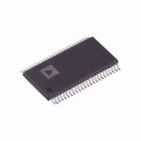
Thin Shrink Small Outline Package [TSSOP PIN 1 0.15 0.05 REV. A OUTLINE DIMENSIONS (RV-48) Dimensions shown in millimeters 12.60 12.50 12.40 25 6.20 6.10 6.00 8.10 BSC 24 1.20 MAX 8 0.5 0 0.27 SEATING 0.20 ...

Page 20

AD5582/AD5583 Revision History Location 8/03—Data Sheet changed from REV REV. A. Change to Figure ...

Related keywords