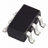
AD5310BRTZ-500RL7 Analog Devices Inc, AD5310BRTZ-500RL7 Datasheet - Page 9

AD5310BRTZ-500RL7
Manufacturer Part Number
AD5310BRTZ-500RL7
Description
IC DAC 10BIT R-R W/BUFF SOT23-6
Manufacturer
Analog Devices Inc
Datasheet
1.AD5310BRMZ.pdf
(12 pages)
Specifications of AD5310BRTZ-500RL7
Data Interface
Serial
Settling Time
6µs
Number Of Bits
10
Number Of Converters
1
Voltage Supply Source
Single Supply
Power Dissipation (max)
1.25mW
Operating Temperature
-40°C ~ 105°C
Mounting Type
Surface Mount
Package / Case
SOT-23-6
Resolution (bits)
10bit
Sampling Rate
167kSPS
Input Channel Type
Serial
Supply Voltage Range - Analog
2.7V To 5.5V
Supply Current
140µA
Digital Ic Case Style
SOT-23
Lead Free Status / RoHS Status
Lead free / RoHS Compliant
Available stocks
Company
Part Number
Manufacturer
Quantity
Price
Company:
Part Number:
AD5310BRTZ-500RL7
Manufacturer:
ADI
Quantity:
3 000
Part Number:
AD5310BRTZ-500RL7
Manufacturer:
ADI/亚德诺
Quantity:
20 000
SYNC Interrupt
In a normal write sequence, the SYNC line is kept low for at
least 16 falling edges of SCLK and the DAC is updated on the
16th falling edge. However, if SYNC is brought high before the
16th falling edge this acts as an interrupt to the write sequence.
The shift register is reset and the write sequence is seen as
invalid. Neither an update of the DAC register contents or a
change in the operating mode occurs—see Figure 23.
Power-On-Reset
The AD5310 contains a power-on-reset circuit which controls
the output voltage during power-up. The DAC register is filled
with zeros and the output voltage is 0 V. It remains there until
a valid write sequence is made to the DAC. This is useful in
applications where it is important to know the state of the out-
put of the DAC while it is in the process of powering up.
Power-Down Modes
The AD5310 contains four separate modes of operation. These
modes are software-programmable by setting two bits (DB13
and DB12) in the control register. Table I shows how the state
of the bits corresponds to the mode of operation of the device.
DB13
0
0
1
1
When both bits are set to 0, the part works normally with its
normal power consumption of 140 A at 5 V. However, for the
three power-down modes, the supply current falls to 200 nA at
5 V (50 nA at 3 V). Not only does the supply current fall but
the output stage is also internally switched from the output of
the amplifier to a resistor network of known values. This has the
advantage that the output impedance of the part is known
while the part is in power-down mode. There are three differ-
ent options. The output is connected internally to GND through a
1 k resistor, a 100 k resistor or it is left open-circuited (Three-
State). The output stage is illustrated in Figure 24.
REV. A
SYNC
SCLK
DIN
Table I. Modes of Operation for the AD5310
SYNC HIGH BEFORE 16
0
1
0
1
DB12
DB15
INVALID WRITE SEQUENCE:
TH
FALLING EDGE
Operating Mode
Normal Operation
Power-Down Modes
DB0
1 k to GND
100 k to GND
Three-State
Figure 23. SYNC Interrupt Facility
–9–
The bias generator, the output amplifier, the resistor string and
other associated linear circuitry are all shut down when the
power-down mode is activated. However, the contents of the
DAC register are unaffected when in power-down. The time to
exit power-down is typically 2.5 s for V
V
MICROPROCESSOR INTERFACING
AD5310 to ADSP-2101/ADSP-2103 Interface
Figure 25 shows a serial interface between the AD5310 and the
ADSP-2101/ADSP-2103. The ADSP-2101/ADSP-2103 should
be set up to operate in the SPORT Transmit Alternate Framing
Mode. The ADSP-2101/ADSP-2103 SPORT is programmed
through the SPORT control register and should be configured as
follows: Internal Clock Operation, Active Low Framing, 16-Bit
Word Length. Transmission is initiated by writing a word to the
Tx register after the SPORT has been enabled.
DD
*ADDITIONAL PINS OMITTED FOR CLARITY
Figure 25. AD5310 to ADSP-2101/ADSP-2103 Interface
= 3 V. See Figure 18 for a plot.
ADSP-2103*
ADSP-2101/
Figure 24. Output Stage During Power-Down
VALID WRITE SEQUENCE, OUTPUT UPDATES
STRING DAC
RESISTOR
DB15
ON THE 16
SCLK
TFS
DT
POWER-DOWN
TH
CIRCUITRY
FALLING EDGE
AMPLIFIER
DB0
DD
= 5 V and 5 s for
RESISTOR
NETWORK
DIN
SCLK
AD5310
AD5310*
V
OUT


