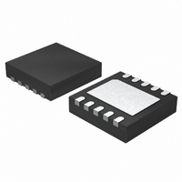
LTC2642AIDD-16#PBF Linear Technology, LTC2642AIDD-16#PBF Datasheet - Page 17

LTC2642AIDD-16#PBF
Manufacturer Part Number
LTC2642AIDD-16#PBF
Description
IC DAC 16BIT VOUT 10-DFN
Manufacturer
Linear Technology
Datasheet
1.LTC2642CDD-12PBF.pdf
(24 pages)
Specifications of LTC2642AIDD-16#PBF
Settling Time
1µs
Number Of Bits
16
Data Interface
Serial
Number Of Converters
1
Voltage Supply Source
Single Supply
Power Dissipation (max)
600µW
Operating Temperature
-40°C ~ 85°C
Mounting Type
Surface Mount
Package / Case
10-DFN
Lead Free Status / RoHS Status
Lead free / RoHS Compliant
Available stocks
Company
Part Number
Manufacturer
Quantity
Price
APPLICATIONS INFORMATION
Op Amp Specifi cations and Bipolar DAC Accuracy
The op amp contributions to unipolar DAC error discussed
above apply equally to bipolar operation. The bipolar ap-
plication circuit gains up the DAC span, and all errors, by
a factor of 2. Since the LSB size also doubles, the errors
in LSBs are identical in unipolar and bipolar modes.
One added error in bipolar mode comes from I
which fl ows through R
bias current offset error becomes:
So:
Settling Time with Op Amp Buffer
When using an external op amp, the output settling time
will still include the single pole settling on the LTC2641/
LTC2642 V
C
the buffer input capacitance and PC board interconnect
capacitance.
The external buffer amplifi er adds another pole to the output
response, with a time constant equal to (fbandwidth/2π).
For example, assume that C
value as above, so that the V
83ns = 1μs/12. The output amplifi er pole will also have a
time constant of 83ns if the closed-loop bandwidth equals
(1/2π • 83ns) = 1.9MHz. The effective time constant of
two cascaded single-pole sections is approximately the
root square sum of the individual time constants, or √2
• 83ns = 117ns, and 1/2 LSB settling time will be ~12 •
117ns = 1.4μs. This represents an ideal case, with no slew
limiting and ideal op amp phase margin. In practice, it
will take a considerably faster amplifi er, as well as careful
attention to maintaining good phase margin, to approach
the unbuffered settling time of 1μs.
The output settling time for bipolar applications (Figure 3)
will be somewhat increased due to the feedback resistor
network R
capacitance, C
a feedback loop pole with a time constant of (C
V
L
OFFSET
) (see Unbuffered V
V
OFFSET
=
FB
(
= (I
OUT
I IN
B
and R
(
P
B
, on the op amp (–) input node will introduce
node, with time constant R
(IN
–
) •
INV
–
) • R
28
OUT
(each 28k nominal). The parasitic
k I IN
FB
FB
– (
to generate an offset. The full
Settling Time). C
B
– I
L
OUT
B
is maintained at the same
+
(IN
) •
node time constant is
+
12 4
) • R
.
k
OUT
)
•
OUT
L
V
• 2) [Volts]
33
will include
REF
P
• (C
k
• 28k/2).
B
[
(IN
LSB
OUT
–
),
]
+
A small feedback capacitor, C1, should be included, to
introduce a zero that will partially cancel this pole. C1
should nominally be <C
to 10pF . This will restore the phase margin and improve
coarse settling time, but a pole-zero doublet will unavoid-
ably leave a slower settling tail, with a time constant of
roughly (C
time to be greater than 2μs.
Reference and GND Input
The LTC2641/LTC2642 operates with external voltage
references from 2V to V
gain errors are virtually unchanged vs V
performance can be maintained if appropriate guidelines
are followed when selecting and applying the reference.
The LTC2641/LTC2642’s very low gain error tempco of
0.1ppm/°C, typical, corresponds to less than 0.5LSB
variation over the –40°C to 85°C temperature range. In
practice, this means that the overall gain error tempco
will be determined almost entirely by the external refer-
ence tempco.
The DAC voltage-switching mode “inverted” resistor ladder
architecture used in the LTC2641/LTC2642 exhibits a refer-
ence input resistance (R
the Typical Performance curves I
In unipolar mode, the minimum R
871Chex, 34,588 decimal) and the the maximum R
300k at code 0000hex (zero scale). The maximum change
in I
occurs near midscale, the INL error is about one half of the
change on V
requires a reference load regulation of (1.53ppm • 2/160μA)
= 19 [ppm/mA]. This implies a reference output impedance
of 48mΩ, including series wiring resistance.
To prevent output glitches from occuring when resistor
ladder branches switch from GND to V
input must maintain low impedance at higher frequencies.
A 0.1μF ceramic capacitor with short leads between REF
and GND provides high frequency bypassing. A surface
mount ceramic chip capacitor is preferred because it has
the lowest inductance. An additional 1μF between REF
and GND provides low frequency bypassing. The circuit
will benefi t from even higher bypass capacitance, as long
REF
for a 2.5V reference is 160μA. Since the maximum
P
+ C1) • 28k/2, which will limit 16-bit settling
REF
, so maintaining an INL error of <0.1LSB
LTC2641/LTC2642
REF
P
, typically in the range of 5pF
DD
) that is code dependent (see
, and linearity, offset and
REF
REF
vs Input Code).
REF
is 14.8k (at code
REF
, the reference
. Full 16-bit
17
REF
26412fb
is


