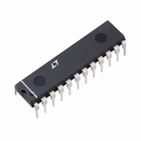
LTC1450CN Linear Technology, LTC1450CN Datasheet - Page 7

LTC1450CN
Manufacturer Part Number
LTC1450CN
Description
IC D/A CONV 12BIT R-R PAR 24-DIP
Manufacturer
Linear Technology
Datasheet
1.LTC1450CGPBF.pdf
(16 pages)
Specifications of LTC1450CN
Settling Time
14µs
Number Of Bits
12
Data Interface
Parallel
Number Of Converters
1
Voltage Supply Source
Single Supply
Power Dissipation (max)
2mW
Operating Temperature
0°C ~ 70°C
Mounting Type
Through Hole
Package / Case
24-DIP (0.300", 7.62mm)
Lead Free Status / RoHS Status
Contains lead / RoHS non-compliant
Available stocks
Company
Part Number
Manufacturer
Quantity
Price
Company:
Part Number:
LTC1450CN#PBF
Manufacturer:
LT
Quantity:
3 400
WR (Pin 1): Write Input (Active Low). Used with CSMSB
and/or CSLSB to load data into the input latches. While WR
and CSMSB and/or CSLSB are held low the enabled input
latches are transparent. The rising edge of WR will latch
data into all input latches.
CSLSB (Pin 2): Chip Select Least Significant Byte (Active
Low). Used with WR to load data into the eight LSB input
latches. While WR and CSLSB are held low the eight LSB
input latches are transparent. The rising edge will latch
data into the eight LSB input latches. Can be connected to
CSMSB for simultaneous loading of both sets of input
latches on a 12-bit bus.
CSMSB (Pin 3): Chip Select Most Significant Byte (Active
Low). Used with WR to load data into the four MSB input
latches. While WR and CSMSB are held low the four MSB
input latches are transparent. The rising edge will latch
data into the four MSB input latches. Can be connected to
CSLSB for simultaneous loading of both sets of input
latches on a 12-bit bus.
D0 to D7 (Pins 4 to 11): Input data for the Least Significant
Byte. Loaded into LSB input latch when WR = 0 and
CSLSB = 0.
D8, D9, D10, D11 (Pins 12, 13, 14, 15): Input data for the
Most Significant Byte. Loaded into MSB input latch when
WR = 0 and CSMSB = 0. Can be connected to D0 to D3 for
multiplexed operation on an 8-bit bus.
GND (Pin 16): Ground.
REFLO (Pin 17): Lower input terminal of the DAC’s inter-
nal resistor string. Typically connected to Analog Ground.
PIN
U
FUNCTIONS
U
U
An input code of (000
the output buffer to this end. Can be used to offset the zero
scale above ground.
REFHI (Pin 18): Upper input terminal of the DAC’s internal
resistor string. Typically connected to REFOUT. An input
code of (FFF
buffer to 1LSB from this end.
REFOUT (Pin 19): Output of the internal 2.048V/1.22V
reference. Typically connected to REFHI to drive internal
DAC resistor string.
V
5.5V (LTC1450) and 2.7V
Requires a bypass capacitor to ground.
V
X1/X2 (Pin 22): Gain Setting Resistor Pin. Connect to GND
for G = 2 or to V
low impedance source, such as ground or V
stability of the output buffer when driving capacitive loads.
CLR (Pin 23): Clear Input (Asynchronous Active Low). A
low on this pin asynchronously resets all internal latches
to 0s.
LDAC (Pin 24): Load DAC (Asynchronous Active Low).
Used to asynchronously transfer the contents of the input
latches to the DAC latches which updates the output
voltage. The rising edge latches the data into the DAC
latches. If held low the DAC latches are transparent and
data from the input latches will immediately update V
CC
OUT
(Pin 20): Positive Power Supply Input. 4.5V V
(Pin 21): Buffered DAC Output.
H
) will connect the positive input of the output
OUT
for G = 1. Should always be tied to a
LTC1450/LTC1450L
H
) will connect the positive input of
V
CC
5.5V (LTC1450L).
OUT
, to ensure
CC
OUT
7
.


