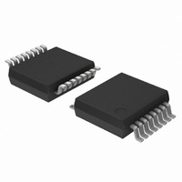
UDA1330ATS/N2,112 NXP Semiconductors, UDA1330ATS/N2,112 Datasheet - Page 14

UDA1330ATS/N2,112
Manufacturer Part Number
UDA1330ATS/N2,112
Description
IC AUDIO DAC STEREO 16-SSOP
Manufacturer
NXP Semiconductors
Datasheet
1.UDA1330ATSN2118.pdf
(23 pages)
Specifications of UDA1330ATS/N2,112
Number Of Bits
20
Data Interface
Serial
Number Of Converters
2
Voltage Supply Source
Analog and Digital
Power Dissipation (max)
75mW
Operating Temperature
-40°C ~ 85°C
Mounting Type
Surface Mount
Package / Case
16-SSOP
Lead Free Status / RoHS Status
Lead free / RoHS Compliant
Settling Time
-
Other names
568-3442-5
935262880112
UDA1330ATSDK
935262880112
UDA1330ATSDK
NXP Semiconductors
Notes
1. All supply connections must be made to the same external power supply unit.
2. The digital input pads are TTL compatible at 5 V, but the pads are not 5 V tolerant in the voltage range between
3. When the DAC drives a capacitive load above 50 pF, a series resistance of 100 Ω must be used to prevent
AC CHARACTERISTICS
f
2001 Feb 02
i
DAC
V
I
R
R
C
Digital-to-analog converter (V
V
ΔV
(THD + N)/S total harmonic distortion-plus-noise to
S/N
α
Digital-to-analog converter (V
V
ΔV
(THD + N)/S total harmonic distortion-plus-noise to
S/N
α
PSRR
o(max)
= 1 kHz; T
cs
cs
SYMBOL
ref(DAC)
SYMBOL
o(rms)
o(rms)
Low-cost stereo filter DAC
o
L
L
o
o
2.7 and 4.5 V.
oscillations in the output operational amplifier.
amb
reference voltage
maximum output current
output resistance
load resistance
load capacitance
output voltage (RMS value)
unbalance between channels
signal ratio
signal-to-noise ratio
channel separation
output voltage (RMS value)
unbalance between channels
signal ratio
signal-to-noise ratio
channel separation
power supply ripple rejection
= 25 °C; R
PARAMETER
L
PARAMETER
= 5 kΩ; all voltages referenced to ground (pins V
DDA
DDA
= V
= V
DDD
DDD
with respect to V
(THD + N)/S < 0.1%;
R
note 3
= 5.0 V)
= 3.3 V)
L
= 5 kΩ
CONDITIONS
at 0 dB
at −60 dB; A-weighted
code = 0; A-weighted
at 0 dB
at −60 dB; A-weighted
code = 0; A-weighted
f
V
ripple
ripple
14
SSA
CONDITIONS
= 1 kHz;
= 100 mV (p-p)
0.45V
−
−
3
−
MIN.
DDA
SSA
and V
0.5V
0.36
0.15
−
−
1.45
0.1
−90
−40
100
100
1.0
0.1
−85
−38
100
100
60
TYP.
TYP.
SSD
DDA
); unless otherwise specified.
0.55V
−
2.0
−
50
−
−
−85
−35
95
−
−
−
−
−
−
−
−
UDA1330ATS
MAX.
MAX.
Product specification
DDA
V
mA
Ω
kΩ
pF
V
dB
dB
dB
dB
dB
V
dB
dB
dB
dB
dB
dB
UNIT
UNIT


