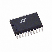
LTC7545AKSW#PBF Linear Technology, LTC7545AKSW#PBF Datasheet - Page 3

LTC7545AKSW#PBF
Manufacturer Part Number
LTC7545AKSW#PBF
Description
IC D/A CONV 12BIT PARALLEL20SOIC
Manufacturer
Linear Technology
Datasheet
1.LTC7545AKSWPBF.pdf
(8 pages)
Specifications of LTC7545AKSW#PBF
Settling Time
1µs
Number Of Bits
12
Data Interface
Parallel
Number Of Converters
1
Voltage Supply Source
Single Supply
Power Dissipation (max)
550µW
Operating Temperature
0°C ~ 70°C
Mounting Type
Surface Mount
Package / Case
20-SOIC (7.5mm Width)
Resolution (bits)
12bit
Input Channel Type
Parallel
Supply Current
2mA
Digital Ic Case Style
SOIC
No. Of Pins
20
Operating Temperature Range
0°C To +70°C
Msl
MSL 1 - Unlimited
Rohs Compliant
Yes
Lead Free Status / RoHS Status
Lead free / RoHS Compliant
Available stocks
Company
Part Number
Manufacturer
Quantity
Price
V
SYMBOL
Digital Inputs
V
V
I
C
Timing Characteristics (Note 3)
t
t
t
t
t
Power Supply
V
I
V
SYMBOL
Digital Inputs
V
V
I
C
Timing Characteristics (Note 3)
t
t
t
t
t
Power Supply
V
I
The
temperature range.
Note 1: 0.5LSB = 0.012% of full scale.
Note 2: Using internal feedback resistor.
Note 3: Guaranteed by design, not subject to test.
Note 4: I
ELECTRICAL CHARACTERISTICS
IN
CS
CH
WR
DS
DH
DD
IN
CS
CH
WR
DS
DH
DD
IH
IL
IN
DD
IH
IL
IN
DD
DD
DD
= 15V, V
= 5V, V
denotes specificatons which apply over the full operating
OUT1
REF
with DAC register loaded to all 0s.
REF
PARAMETER
Digital Input High Voltage
Digital Input Low Voltage
Digital Input Current
Digital Input Capacitance
CS to WR Setup Time
CS to WR Hold Time
Write Pulse Width
Data Setup Time
Data Hold Time
Supply Voltage
Supply Current
PARAMETER
Digital Input High Voltage
Digital Input Low Voltage
Digital Input Current
Digital Input Capacitance
CS to WR Setup Time
CS to WR Hold Time
Write Pulse Width
Data Setup Time
Data Hold Time
Supply Voltage
Supply Current
= 10V, V
= 10V, V
OUT1
OUT1
= AGND = 0V, T
= AGND = 0V, T
A
A
= T
= T
MIN
MIN
to T
CONDITIONS
(Note 3) V
All Digital Inputs = V
All Digital Inputs = 0V or V
CONDITIONS
(Note 3) V
All Digital Inputs = V
All Digital Inputs = 0V or V
to T
MAX,
MAX,
unless otherwise noted.
IN
IN
unless otherwise noted.
= 0V
= 0V
Note 5: Typical temperature coefficient is 100ppm/ C.
Note 6: OUT1 load = 100 in parallel with 13pF.
Note 7: To 0.01% for a full-scale change, measured from the falling
edge of WR, CS = 0V.
Note 8: From digital input change to 90% of final analog output.
Note 9: V
or all 1s to all 0s.
IH
IH
or V
or V
DD
DD
IL
IL
REF
= 0V. DAC register contents changed from all 0s to all 1s
14.25
MIN
4.75
MIN
13.5
100
100
100
2.4
75
75
60
0
5
0
5
ALL GRADES
ALL GRADES
0.001
TYP
TYP
10
15
10
5
LTC7545A
15.75
MAX
MAX
5.25
100
100
0.8
1.5
8
2
8
2
1
1
UNITS
UNITS
3
mA
mA
pF
ns
ns
ns
ns
ns
pF
ns
ns
ns
ns
ns
V
V
A
V
A
V
V
A
V
A


