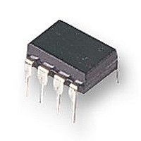
HCPL-2531 Fairchild Semiconductor, HCPL-2531 Datasheet - Page 6

HCPL-2531
Manufacturer Part Number
HCPL-2531
Description
OPTOCOUPLER, DUAL, TRANSISTOR O/P
Manufacturer
Fairchild Semiconductor
Datasheet
1.6N136.S.pdf
(12 pages)
Specifications of HCPL-2531
No. Of Channels
2
Isolation Voltage
2.5kV
Optocoupler Output Type
Phototransistor
Input Current
16mA
Output Voltage
20V
Opto Case Style
DIP
No. Of Pins
8
Svhc
No SVHC (15-Dec-2010)
Approval
RoHS Compliant
Rohs Compliant
Yes
Available stocks
Company
Part Number
Manufacturer
Quantity
Price
Company:
Part Number:
HCPL-2531
Manufacturer:
AVAGO
Quantity:
40 000
Part Number:
HCPL-2531
Manufacturer:
AGILENT
Quantity:
20 000
Company:
Part Number:
HCPL-2531#300E
Manufacturer:
AVAGO
Quantity:
10 000
Company:
Part Number:
HCPL-2531-000E
Manufacturer:
PANASONIC
Quantity:
2 000
Company:
Part Number:
HCPL-2531-000E
Manufacturer:
AVAGO
Quantity:
40 000
Part Number:
HCPL-2531-000E
Manufacturer:
AVAGO/安华高
Quantity:
20 000
Company:
Part Number:
HCPL-2531-020E
Manufacturer:
AVAGO
Quantity:
12 000
Single-channel: 6N135, 6N136 , HCPL-2503, HCPL-4502 Dual-Channel: HCPL-2530, HCPL-2531 Rev. 1.0.3
Isolation Characteristics
Notes
1.
2.
3.
4.
5.
6.
7.
8.
10. Measured between pins 1 and 2 shorted together, and pins 3 and 4 shorted together.
I
9. Device is considered a two terminal device: Pins 1, 2, 3 and 4 are shorted together and Pins 5, 6, 7 and 8 are shorted together.
Characteristics
Input-output
insulation leakage current
Withstand insulation test voltage
Resistance (input to output)
Capacitance (input to output)
DC Current gain
Input-Input
Insulation leakage current
Input-Input Resistance
Input-Input Capacitance
Derate linearly above 70°C free-air temperature at a rate of 0.8 mA/°C.
Derate linearly above 70°C free-air temperature at a rate of 1.6 mA/°C.
Derate linearly above 70°C free-air temperature at a rate of 0.9 mW/°C.
Derate linearly above 70°C free-air temperature at a rate of 2.0 mW/°C.
Current Transfer Ratio is defined as a ratio of output collector current, I
The 4.1 kΩ load represents 1 LSTTL unit load of 0.36 mA and 6.1kΩ pull-up resistor.
The 1.9 kΩ load represents 1 TTL unit load of 1.6 mA and 5.6 kΩ pull-up resistor.
Common mode transient immunity in logic high level is the maximum tolerable (positive) dV
mon mode pulse signal V
immunity in logic low level is the maximum tolerable (negative) dV
V
CM
, to assure that the output will remain in a logic low state (i.e., V
CM
, to assure that the output will remain in a logic high state (i.e., V
(RH ≤ 45%, V
(T
A
t = 5 s, (HCPL-2530/2531 only)
= 0 to 70°C Unless otherwise specified)
Test Conditions
(V
(Note 9) (V
(Relative humidity = 45%)
I-I
I-I
(HCPL-2530/2531 only)
(HCPL-2530/2531 only)
(RH ≤ 50%, T
= 500 VDC) (Note 10)
= 500 VDC) (Note 10)
(I
(f = 1 MHz) (Note 10)
(Note 9) ( t = 1 min.)
(Note 9) (f = 1 MHz)
O
(T
(V
= 3 mA, V
A
I-O
= 25°C, t = 5 s)
I-O
= 3000 VDC)
= 500 VDC)
6
A
(Note 9)
O
= 25°C)
= 5 V)
cm
O
/dt on the trailing edge of the common mode pulse signal,
<0.8 V).
O
, to the forward LED input current, I
Symbol
V
HFE
R
C
I
R
C
I
I-O
ISO
I-O
I-O
I-I
I-I
I-I
Min
2500
cm
O
/dt on the leading edge of the com-
>2.0 V). Common mode transient
Typ**
0.005
10
10
0.03
150
0.6
12
11
F
, times 100%.
Max
1.0
www.fairchildsemi.com
V
Unit
µA
RMS
pF
µA
pF
Ω
Ω


