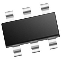
PIC10F222-I/OT Microchip Technology, PIC10F222-I/OT Datasheet - Page 34

PIC10F222-I/OT
Manufacturer Part Number
PIC10F222-I/OT
Description
768B Flash, 23B RAM, 4 I/O, 8bit ADC 6 SOT-23 BAG
Manufacturer
Microchip Technology
Series
PIC® 10Fr
Datasheet
1.PIC10F220-IMC.pdf
(86 pages)
Specifications of PIC10F222-I/OT
Processor Series
PIC10F
Core
RISC
Data Bus Width
8 bit
Program Memory Type
Flash
Program Memory Size
512 B
Data Ram Size
23 B
Interface Type
RS-232, USB
Maximum Clock Frequency
8 MHZ
Number Of Programmable I/os
4
Number Of Timers
1
Maximum Operating Temperature
+ 85 C
Mounting Style
SMD/SMT
Package / Case
SOT-23-6
Operating Temperature Range
- 40 C to + 85 C
Processor To Be Evaluated
PIC10F222
Supply Current (max)
100 nA
Core Processor
PIC
Core Size
8-Bit
Speed
8MHz
Connectivity
-
Peripherals
POR, WDT
Number Of I /o
4
Eeprom Size
-
Ram Size
23 x 8
Voltage - Supply (vcc/vdd)
2 V ~ 5.5 V
Data Converters
A/D 2x8b
Oscillator Type
Internal
Operating Temperature
-40°C ~ 85°C
Lead Free Status / Rohs Status
Details
PIC10F220/222
7.9
For the ADC to meet its specified accuracy, the charge
holding capacitor (C
charge to the input channel voltage level. The Analog
Input model is shown in Figure 7-1. The source
impedance (R
impedance directly affect the time required to charge the
capacitor C
varies over the device voltage (V
The maximum recommended impedance for analog
sources is 10 kΩ. As the source impedance is
decreased, the acquisition time may be decreased.
EQUATION 7-1:
FIGURE 7-1:
DS41270E-page 32
Assumptions:
Solving for Tc:
Therefore:
Note 1: The charge holding capacitor (C
Legend:
2: The maximum recommended impedance for analog sources is 10 kΩ. This is required to meet the pin
A/D Acquisition Requirements
HOLD
leakage specification.
S
CPIN
V
I
R
SS
C
LEAKAGE
) and the internal sampling switch (R
T
IC
HOLD
. The sampling switch (R
Temperature = 50°C and external impedance of 10 k
Tacq
Tc
Tacq
HOLD
VA
ACQUISITION TIME EXAMPLE
ANALOG INPUT MODULE
Rs
= Input Capacitance
= Threshold Voltage
= Leakage current at the pin due
= Interconnect Resistance
= Sampling Switch
= Sample/Hold Capacitance
) must be allowed to fully
to various junctions
= Amplifier Settling Time + Hold Capacitor Charging Time + Temperature Coefficient
= T
= 2
= C
= -25pF (l k
= 2.81
= 2
= 6.06
ANx
C
5 pF
PIN
AMP
HOLD
μ
μ
DD
s + T
s + 2.81
μ
μ
), see Figure 7-1.
+ T
s
s
(R
C
SS
C
Ω
IC
+ [(Temperature - 25°C)(0.05
+ T
) impedance
μ
+ 7 k
+ R
s + [(50°C-25°C)(0.0 5
HOLD
COFF
V
SS
DD
Ω
V
+ R
V
) is not discharged after each conversion.
+ 10 k
T
T
SS
= 0.6V
= 0.6V
S
) In(1/512)
)
Ω
) In(0.00196)
I
± 500 nA
R
LEAKAGE
After the analog input channel is selected (or changed),
an A/D acquisition must be done before the conversion
can be started. To calculate the minimum acquisition
time, Equation 7-1 may be used. This equation
assumes that 1/2 LSb error is used (256 steps for the
ADC). The 1/2 LSb error is the maximum error allowed
for the ADC to meet its specified resolution.
IC
Ω
μ
s/°C)]
≤ 1k
5.0V V
μ
s/°C)]
V
DD
SS Rss
DD
Sampling
Switch
6V
5V
4V
3V
2V
Sampling Switch
5 6 7 8 9 10 11
C
© 2007 Microchip Technology Inc.
V
(kΩ)
HOLD
SS
R
/V
SS
REF
= 25 pF
-


