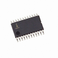
X9408WV24 Intersil, X9408WV24 Datasheet - Page 6

X9408WV24
Manufacturer Part Number
X9408WV24
Description
IC DCP QUAD 10K 64TP 24TSSOP
Manufacturer
Intersil
Series
XDCP™r
Datasheet
1.X9408WS24I.pdf
(20 pages)
Specifications of X9408WV24
Taps
64
Resistance (ohms)
10K
Number Of Circuits
4
Temperature Coefficient
300 ppm/°C Typical
Memory Type
Non-Volatile
Interface
I²C, 2-Wire Serial
Voltage - Supply
4.5 V ~ 5.5 V
Operating Temperature
0°C ~ 70°C
Mounting Type
Surface Mount
Package / Case
24-TSSOP
Resistance In Ohms
10K
Lead Free Status / RoHS Status
Contains lead / RoHS non-compliant
Available stocks
Company
Part Number
Manufacturer
Quantity
Price
Part Number:
X9408WV24I
Manufacturer:
INTERSIL
Quantity:
20 000
Part Number:
X9408WV24Z-2.7T1
Manufacturer:
INTERSIL
Quantity:
20 000
The Increment/Decrement command is different from the
other commands. Once the command is issued and the
X9408 has responded with an acknowledge, the master can
clock the selected wiper up and/or down in one segment
steps; thereby, providing a fine tuning capability to the host.
For each SCL clock pulse (t
NOTE: (7)1/0 = data is one or zero
Read Wiper CounterRegister
Write Wiper CounterRegister
Read Data Register
Write Data Register
XFR Data Register to Wiper
Counter Register
XFR Wiper Counter Register
to Data Register
Global XFR Data Registers
to Wiper Counter Registers
Global XFR Wiper Counter
Registers to Data Register
Increment/Decrement Wiper
Counter Register
SCL
SDA
SCL
SDA
INSTRUCTION
S
T
A
R
T
S
T
A
R
T
0
0
1
1
0
0
1
1
HIGH
A3 A2 A1 A0
I
1
1
1
1
1
1
0
1
0
3
6
A3
) while SDA is HIGH, the
FIGURE 5. INCREMENT/DECREMENT INSTRUCTION SEQUENCE
I
0
0
0
1
1
1
0
0
0
2
A2
A1
I
0
1
1
0
0
1
0
0
1
FIGURE 4. THREE-BYTE INSTRUCTION SEQUENCE
1
INSTRUCTION SET
A0
A
C
K
I
1
0
1
0
1
0
1
0
0
0
I3
A
C
K
R
R
R
R
R
R
R
0
0
0
TABLE 1. INSTRUCTION SET
1
1
1
1
1
1
1
I3
I2
R
R
R
R
R
R
R
0
0
0
I2
0
0
0
0
0
0
0
I1
X9408
I0
P
P
P
P
P
P
P
P
I1
0
0
1
1
1
1
1
1
1
1
R1 R0 P1 P0
I0
P
P
P
P
P
P
P
P
0
0
0
0
0
0
0
0
0
0
selected wiper will move one resistor segment towards the
R
LOW, the selected wiper will move one resistor segment
towards the R
sequence and timing for this operation are shown in Figures
5 and 6 respectively.
R1
H
Read the contents of the Wiper Counter Register pointed to by
P
Write new value to the Wiper Counter Register pointed to by P
Read the contents of the Data Register pointed to by P
R
Write new value to the Data Register pointed to by
P
Transfer the contents of the Data Register pointed to by P
and R
Transfer the contents of the Wiper Counter Register pointed to by
P
Transfer the contents of the Data Registers pointed to by R
of all four pots to their respective Wiper Counter Registers
Transfer the contents of both Wiper Counter Registers to their
respective Data Registers pointed to by
R
Enable Increment/decrement of the Wiper Counter Register
pointed to by P
terminal. Similarly, for each SCL clock pulse while SDA is
1
1
1
1
1
R0
- P
- P
- P
- R
- R
1
0
0
0
0
0
P1
- R
and R
to the Data Register pointed to by R
of all four pots
A
C
K
0
P0
L
to its associated Wiper Counter Register
1
terminal. A detailed illustration of the
0
1
- R
- P
A
C
K
0
0
0
N
C
1
I
D5 D4
OPERATION
N
C
2
I
D3 D2
N
C
n
I
D
E
C
1
D1 D0
1
- R
0
D
E
C
January 15, 2009
n
A
C
K
1
- P
S
T
O
P
S
T
O
P
FN8191.4
1
1
0
1
- P
- R
and
- P
0
0
0


