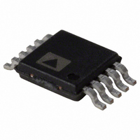
AD5161BRM5 Analog Devices Inc, AD5161BRM5 Datasheet - Page 12

AD5161BRM5
Manufacturer Part Number
AD5161BRM5
Description
IC POT DGTL 5K 256POS 10-MSOP
Manufacturer
Analog Devices Inc
Datasheet
1.AD5161BRMZ10.pdf
(20 pages)
Specifications of AD5161BRM5
Rohs Status
RoHS non-compliant
Taps
256
Resistance (ohms)
5K
Number Of Circuits
1
Temperature Coefficient
45 ppm/°C Typical
Memory Type
Volatile
Interface
I²C, SPI
Voltage - Supply
2.7 V ~ 5.5 V
Operating Temperature
-40°C ~ 125°C
Mounting Type
Surface Mount
Package / Case
10-MSOP, Micro10™, 10-uMAX, 10-uSOP
Resistance In Ohms
5K
Number Of Elements
1
# Of Taps
256
Resistance (max)
5KOhm
Power Supply Requirement
Single
Single Supply Voltage (typ)
3/5V
Dual Supply Voltage (typ)
Not RequiredV
Single Supply Voltage (min)
2.7V
Single Supply Voltage (max)
5.5V
Dual Supply Voltage (min)
Not RequiredV
Dual Supply Voltage (max)
Not RequiredV
Operating Temp Range
-40C to 125C
Operating Temperature Classification
Automotive
Mounting
Surface Mount
Pin Count
10
Lead Free Status / RoHS Status
Not Compliant
Available stocks
Company
Part Number
Manufacturer
Quantity
Price
Part Number:
AD5161BRM50
Manufacturer:
ADI/亚德诺
Quantity:
20 000
AD5161
TEST CIRCUITS
Figure 28 to Figure 36 illustrate the test circuits that define the test conditions used in the product specification tables.
Figure 28. Test Circuit for Potentiometer Divider Nonlinearity Error (INL, DNL)
Figure 31. Test Circuit for Power Supply Sensitivity (PSS, PSSR)
Figure 29. Test Circuit for Resistor Position Nonlinearity Error
V
V+
MS2
OFFSET
GND
Figure 30. Test Circuit for Wiper Resistance
V
DD
Figure 32. Test Circuit for Inverting Gain
V+
NO CONNECT
(Rheostat Operation; R-INL, R-DNL)
V
A
A
B
A
B
V
DUT
IN
W
W
A
B
DUT
A
A
DUT
B
W
OFFSET
BIAS
W
DUT
V
W
V
W
B
MS1
V
MS
PSRR (dB) = 20 LOG
PSS (%/%) =
V+ = V
I
W
OP279
= V
1LSB = V+/2
V+ = V
V
R
5V
V
MS
DD
DD
W
MS
= [V
/ R
DD
I
10%
W
NOMINAL
MS1
ΔV
ΔV
N
MS
DD
– V
V
%
%
OUT
MS2
(
ΔV
ΔV
]/I
MS
DD
W
)
Rev. A | Page 12 of 20
Figure 36. Test Circuit for Common-Mode Leakage current
OFFSET
Figure 35. Test Circuit for Incremental ON Resistance
GND
OFFSET
Figure 33. Test Circuit for Noninverting Gain
Figure 34. Test Circuit for Gain vs. Frequency
V
GND
V
V
DD
SS
IN
2.5V
DUT
GND
DUT
B
V
W
IN
DUT
OFFSET
BIAS
NC
A
NC
A
B
I
B
A
SW
DUT
W
NC = NO CONNECT
V
SS
CODE = 0x00
W
R
SW
W
TO V
B
=
OP279
0.1V
DD
I
I
SW
5V
CM
AD8610
–15V
+15V
0.1V
V
V
OUT
CM
V
OUT


