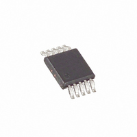
DS3906U+ Maxim Integrated Products, DS3906U+ Datasheet - Page 7

DS3906U+
Manufacturer Part Number
DS3906U+
Description
IC RESIST VAR TRPL 10USOP
Manufacturer
Maxim Integrated Products
Datasheet
1.DS3906U.pdf
(14 pages)
Specifications of DS3906U+
Taps
64
Resistance (ohms)
1.45K, 2.54K, 2.54K
Number Of Circuits
3
Temperature Coefficient
60 ppm/°C Typical
Memory Type
Non-Volatile
Interface
I²C, 2-Wire Serial
Voltage - Supply
2.7 V ~ 5.5 V
Operating Temperature
-40°C ~ 85°C
Mounting Type
Surface Mount
Package / Case
10-MSOP, Micro10™, 10-uMAX, 10-uSOP
Resistance In Ohms
1.45K, 2.54K, 2.54K
Lead Free Status / RoHS Status
Lead free / RoHS Compliant
GND
SDA
SCL
V
A0
CC
A1
A2
PIN
10
1
2
3
4
5
6
7
8
9
INTERFACE
V
(00h-0Fh)
16 BYTES
EEPROM
CC
DS3906
USER
I
2
C
NAME
GND
SDA
SCL
V
A1
H2
H1
H0
A0
A2
CC
F8h
F9h
FAh
MSB
MSB
MSB
RHIZ CONTROL
RHIZ CONTROL
RHIZ CONTROL
EEPROM
I
I
I
Power Supply Voltage
Ground
High Terminal of Resistor 2
High Terminal of Resistor 1
High Terminal of Resistor 0
I
2
2
2
2
RESISTOR 0
RESISTOR 1
RESISTOR 2
C Address Input. Inputs A0, A1, and A2 determine the I
C Serial Data Open-Drain Input/Output
C Serial Clock Input
C Address Input. Inputs A0, A1, and A2 determine the I
6
6
6
Block Diagram
LSB
LSB
LSB
Triple NV Low Step Size Variable
_____________________________________________________________________
RES 0
2.54kΩ
RES 1
2.54kΩ
RES 2
1.45kΩ
H0
H1
H2
The DS3906 contains three variable resistors plus a
user EEPROM. The block diagram illustrates these in
addition to the registers that control the resistors. The
following sections provide detailed information about
the DS3906.
The DS3906 contains 16 bytes of User EEPROM plus 3
NV resistor registers. Refer to Table 1. Communication
with the memory/registers is achieved through the I
compatible serial interface and is described in subse-
quent sections.
Each of the three resistors in the DS3906 has its own
control register used to set the resistor position. Refer
to the block diagram and Table 2. Each resistor has 64
positions plus a high impedance state. The nominal
resistance values for each position is listed in Table 3.
Resistors 0 and 1 have the same full-scale resistance,
which is different than resistor 2. As shown in Table 3,
the resistors have a pseudo-log response (resistance
vs. position) when used without an external parallel
resistor. Valid resistor settings are 00h to 3Fh. Writing a
value greater than 3Fh to any of the resistor registers
Resistor Plus Memory
FUNCTION
2
2
C slave address of the device.
C slave address of the device.
Resistor Registers/Settings
Detailed Description
Memory Organization
Pin Description
2
C-
7


