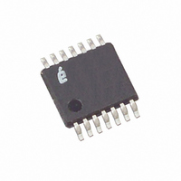
X9111TV14 Intersil, X9111TV14 Datasheet - Page 3

X9111TV14
Manufacturer Part Number
X9111TV14
Description
IC DCP 100K 1024TP 14TSSOP
Manufacturer
Intersil
Series
XDCP™r
Datasheet
1.X9111TV14.pdf
(17 pages)
Specifications of X9111TV14
Taps
1024
Resistance (ohms)
100K
Number Of Circuits
1
Temperature Coefficient
300 ppm/°C Typical
Memory Type
Non-Volatile
Interface
SPI, 3-Wire Serial
Voltage - Supply
4.5 V ~ 5.5 V
Operating Temperature
0°C ~ 70°C
Mounting Type
Surface Mount
Package / Case
14-TSSOP
Resistance In Ohms
100K
Lead Free Status / RoHS Status
Contains lead / RoHS non-compliant
Available stocks
Company
Part Number
Manufacturer
Quantity
Price
Company:
Part Number:
X9111TV1427
Manufacturer:
MAXM
Quantity:
3 513
Part Number:
X9111TV1427
Manufacturer:
INTERSIL
Quantity:
20 000
Company:
Part Number:
X9111TV14IZ-2.7
Manufacturer:
TI
Quantity:
47
Company:
Part Number:
X9111TV14Z
Manufacturer:
Intersil
Quantity:
1
Company:
Part Number:
X9111TV14Z-2.7
Manufacturer:
Intersil
Quantity:
1 425
Part Number:
X9111TV14Z-2.7
Manufacturer:
INTERSIL
Quantity:
20 000
Pin Descriptions
Pin Descriptions
Bus Interface Pins
SERIAL OUTPUT (SO)
SO is a serial data output pin. During a read cycle, data is
shifted out on this pin. Data is clocked out by the falling edge
of the serial clock.
SERIAL INPUT (SI)
SI is the serial data input pin. All opcodes, byte addresses and
data to be written to the pots and pot registers are input on this
pin. Data is latched by the rising edge of the serial clock.
SERIAL CLOCK (SCK)
The SCK input is used to clock data into and out of the
X9111.
HOLD (HOLD)
HOLD is used in conjunction with the CS pin to select the
device. Once the part is selected and a serial sequence is
underway, HOLD may be used to pause the serial
communication with the controller without resetting the serial
sequence. To pause, HOLD must be brought LOW while SCK is
LOW. To resume communication, HOLD is brought HIGH, again
while SCK is LOW. If the pause feature is not used, HOLD should
be held HIGH at all times.
DEVICE ADDRESS (A
The address inputs are used to set the 8-bit slave address. A
match in the slave address serial data stream must be made
with the address input (A1–A0) in order to initiate
communication with the X9111.
(TSSOP)
PIN
10
11
12
13
14
1
2
3
4
5
6
7
8
9
SYMBOL
HOLD
SCK
V
V
WP
R
SO
NC
CS
R
A0
A1
R
SI
SS
CC
W
H
L
0
, A
Serial Data Output
Device Address
No Connect
Chip Select
Serial Clock
Serial Data Input
System Ground
Hardware Write Protect
Device Address
Device Select. Pause the Serial Bus
Wiper Terminal of the Potentiometer
High Terminal of the Potentiometer
Low Terminal of the Potentiometer
System Supply Voltage
1
)
3
FUNCTION
X9111
CHIP SELECT (CS)
When CS is HIGH, the X9111 is deselected and the SO pin is at
high impedance, and (unless an internal write cycle is
underway) the device will be in the standby state. CS LOW
enables the X9111, placing it in the active power mode. It
should be noted that after a power-up, a HIGH to LOW
transition on CS is required prior to the start of any operation.
HARDWARE WRITE PROTECT INPUT (WP)
The WP pin when LOW prevents nonvolatile writes to the
Data Registers.
Potentiometer Pins
R
The R
on a mechanical potentiometer.
R
The wiper pin is equivalent to the wiper terminal of a
mechanical potentiometer.
Bias Supply Pins
SYSTEM SUPPLY VOLTAGE (V
GROUND (V
The V
the system ground.
Other Pins
NO CONNECT (NC)
Pin should be left open. This pin is used for Intersil
manufacturing and test purposes.
Principles of Operation
Device Description
Serial Interface
The X9111 supports the SPI interface hardware conventions.
The device is accessed via the SI input with data clocked-in on
the rising SCK. CS must be LOW and the HOLD and WP pins
must be HIGH during the entire operation.
The SO and SI pins can be connected together, since they
have three state outputs. This can help to reduce system pin
count.
Array Description
The X9111 is comprised of a resistor array (see Figure 1).
The array contains the equivalent of 1023 discrete resistive
segments that are connected in series. The physical ends of
each array are equivalent to the fixed terminals of a
mechanical potentiometer (R
At both ends of each array and between each resistor
segment is a CMOS switch connected to the wiper (R
output. Within the individual array only one switch may be
turned on at a time.
H
W
, R
L
H
CC
and R
pin is the system supply voltage. The V
SS
L
pins are equivalent to the terminal connections
)
H
and R
CC
) AND SUPPLY
L
inputs).
September 15, 2006
SS
pin is
W
FN8159.4
)


