AD5252BRUZ10 Analog Devices Inc, AD5252BRUZ10 Datasheet - Page 4
AD5252BRUZ10
Manufacturer Part Number
AD5252BRUZ10
Description
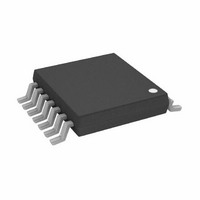
IC DIG POT DUAL 256 10K 14TSSOP
Manufacturer
Analog Devices Inc
Datasheet
1.AD5252BRUZ10.pdf
(28 pages)
Specifications of AD5252BRUZ10
Taps
256
Resistance (ohms)
10K
Number Of Circuits
2
Temperature Coefficient
650 ppm/°C Typical
Memory Type
Non-Volatile
Interface
I²C, 2-Wire Serial
Voltage - Supply
2.7 V ~ 5.5 V, ±2.25 V ~ 2.75 V
Operating Temperature
-40°C ~ 85°C
Mounting Type
Surface Mount
Package / Case
14-TSSOP
Resistance In Ohms
10K
End To End Resistance
10kohm
Track Taper
Linear
Resistance Tolerance
± 20%
No. Of Steps
256
Supply Voltage Range
2.7V To 5.5V, ± 2.25V To ± 2.75V
Control Interface
I2C, Serial
Lead Free Status / RoHS Status
Lead free / RoHS Compliant
For Use With
AD5252EVAL - BOARD EVAL FOR AD5252
Lead Free Status / RoHS Status
Lead free / RoHS Compliant, Lead free / RoHS Compliant
Available stocks
Company
Part Number
Manufacturer
Quantity
Price
Company:

Part Number:
AD5252BRUZ10
Manufacturer:
Renesas
Quantity:
41
Part Number:
AD5252BRUZ10
Manufacturer:
ADI/亚德诺
Quantity:
20 000
Company:
Part Number:
AD5252BRUZ100
Manufacturer:
Analog Devices Inc
Quantity:
135
Company:
Part Number:
AD5252BRUZ100
Manufacturer:
ADI
Quantity:
3 529


AD5251/AD5252
Parameter
DIGITAL INPUTS AND OUTPUTS
POWER SUPPLIES
DYNAMIC CHARACTERISTICS
1
2
3
4
5
6
7
8
Typical values represent average readings at 25°C and V
Resistor position nonlinearity error (R-INL) is the deviation from an ideal value measured between the maximum and minimum resistance wiper positions. R-DNL is the
relative step change from an ideal value measured between successive tap positions. Parts are guaranteed monotonic, except R-DNL of AD5252 1 kΩ version at V
2.7 V, I
INL and DNL are measured at V
DNL specification limits of ±1 LSB maximum are guaranteed monotonic operating conditions.
Resistor Terminal A, Terminal B, and Terminal W have no limitations on polarity with respect to each other.
Guaranteed by design and not subject to production test.
Command 0 NOP should be activated after Command 1 to minimize I
P
All dynamic characteristics use V
DISS
Input Logic High
Input Logic Low
Output Logic High (SDA)
Output Logic Low (SDA)
WP Leakage Current
A0 Leakage Current
Input Leakage Current
Input Capacitance
Single-Supply Power Range
Dual-Supply Power Range
Positive Supply Current
Negative Supply Current
EEMEM Data Storing Mode Current
EEMEM Data Restoring Mode
Power Dissipation
Power Supply Sensitivity
Bandwidth –3 dB
Total Harmonic Distortion
V
Resistor Noise Voltage
Digital Crosstalk
Analog Coupling
W
is calculated from I
(Other than WP and A0)
Current
Settling Time
W
= V
DD
/R for both V
6
DD
7
5
× V
DD
= 3 V and V
DD
W
= 5 V.
DD
with the RDAC configured as a potentiometer divider, similar to a voltage output digital-to-analog converter. V
5, 8
= 5 V.
DD
= 5 V.
Symbol
V
V
V
V
I
I
I
C
V
V
I
I
I
I
P
PSS
BW
THD
t
e
C
C
WP
A0
I
DD
SS
DD_STORE
DD_RESTORE
S
N_WB
IH
IL
OH
OL
DD
DD
DISS
I
T
AT
/V
SS
DD
= 5 V.
DD_READ
Rev. B | Page 4 of 28
Conditions
V
V
V
R
R
WP = V
A0 = GND
V
V
V
V
V
V
V
V
ΔV
ΔV
R
V
V
R
(thermal noise only)
V
adjacent RDAC making full-scale
change
Signal input at A1 and measure the
output at W3, f = 1 kHz
current consumption.
PULL-UP
PULL-UP
DD
DD
DD
IN
SS
IH
IH
SS
IH
IH
IH
AB
A
A
WB
A
DD
DD
= 1 V rms, V
= V
= V
= V
= V
= V
= V
= V
/V
= 0 V or V
= 0 V
= –2.5 V
= 1 kΩ
= 5 V, V
= 5 V, V
= 500 Ω, f = 1 kHz
SS
= 5 V ± 10%
= 3 V ± 10%
DD
DD
DD
DD
DD
DD
DD
= 2.2 kΩ to V
= 2.2 kΩ to V
DD
= 2.7 V/0 V or V
, V
, V
or V
or V
or V
or V
= 5 V or V
B
B
SS
SS
= 0 V
= 0 V, measure V
DD
IL
IL
IL
IL
= 0 V
= 0 V
B
= GND
= GND, V
= GND
= GND
= 0 V, f = 1 kHz
IL
DD
DD
= GND
= 5 V, V
= 5 V, V
DD
DD
/V
SS
= 2.5 V,
= ± 2.5 V
W
SS
SS
with
= 0 V
= 0 V
Min
2.4
2.1
4.9
2.7
±2.25
−0.025
–0.04
Typ
5
5
–5
35
2.5
+0.010
+0.02
4
0.05
0.2
3
–80
–72
1
A
= V
Max
0.8
0.4
5
3
±1
5.5
±2.75
15
–15
0.075
+0.025
+0.04
DD
and V
B
Unit
V
V
V
V
V
μA
μA
μA
pF
V
V
μA
μA
mA
mA
mW
%/%
%/%
MHz
%
μs
nV/√Hz
dB
dB
= 0 V.
DD
=
Related parts for AD5252BRUZ10
Image
Part Number
Description
Manufacturer
Datasheet
Request
R

Part Number:
Description:
±1.7g Dual-Axis IMEMS Accelerometer Evaluation Board
Manufacturer:
Analog Devices Inc
Datasheet:

Part Number:
Description:
Inertial Sensor Evaluation System
Manufacturer:
Analog Devices Inc
Datasheet:
Part Number:
Description:
Manufacturer:
Analog Devices Inc
Datasheet:
Part Number:
Description:
Manufacturer:
Analog Devices Inc
Datasheet:
Part Number:
Description:
Manufacturer:
Analog Devices Inc
Datasheet:
Part Number:
Description:
Manufacturer:
Analog Devices Inc
Datasheet:
Part Number:
Description:
Manufacturer:
Analog Devices Inc
Datasheet:
Part Number:
Description:
Manufacturer:
Analog Devices Inc
Datasheet:
Part Number:
Description:
Manufacturer:
Analog Devices Inc
Datasheet:
Part Number:
Description:
Manufacturer:
Analog Devices Inc
Datasheet:
Part Number:
Description:
Manufacturer:
Analog Devices Inc
Datasheet:
Part Number:
Description:
Manufacturer:
Analog Devices Inc
Datasheet:
Part Number:
Description:
Manufacturer:
Analog Devices Inc
Datasheet: