AD7843ARQZ Analog Devices Inc, AD7843ARQZ Datasheet - Page 6
AD7843ARQZ
Manufacturer Part Number
AD7843ARQZ
Description
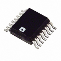
IC ADC 12BIT TOUCHSCREEN 16-QSOP
Manufacturer
Analog Devices Inc
Type
Resistiver
Datasheet
1.AD7843ARUZ.pdf
(20 pages)
Specifications of AD7843ARQZ
Resolution (bits)
12 b
Data Interface
Serial
Touch Panel Interface
4-Wire
Number Of Inputs/keys
1 TSC
Data Rate/sampling Rate (sps, Bps)
125k
Voltage Reference
External
Voltage - Supply
2.2 V ~ 5.25 V
Operating Temperature
-40°C ~ 85°C
Mounting Type
Surface Mount
Package / Case
16-QSOP
Voltage Supply Source
Single Supply
Sampling Rate (per Second)
125k
Sampling Rate
125kSPS
Supply Current
240µA
Digital Ic Case Style
QSOP
No. Of Pins
16
Operating Temperature Range
-40°C To +85°C
Lead Free Status / RoHS Status
Lead free / RoHS Compliant
For Use With
EVAL-AD7843EBZ - BOARD EVAL FOR AD7843
Lead Free Status / RoHS Status
Lead free / RoHS Compliant, Lead free / RoHS Compliant
Available stocks
Company
Part Number
Manufacturer
Quantity
Price

Company:
Part Number:
AD7843ARQZ
Manufacturer:
ADI
Quantity:
196
Part Number:
AD7843ARQZ
Manufacturer:
ADI/亚德诺
Quantity:
20 000


AD7843
PIN CONFIGURATION AND FUNCTION DESCRIPTIONS
Table 4. Pin Function Descriptions
Pin No.
1, 10
2
3
4
5
6
7
8
9
11
12
13
14
15
16
Mnemonic
+V
X+
Y+
X−
Y−
GND
IN3
IN4
V
PENIRQ
DOUT
BUSY
DIN
CS
DCLK
REF
CC
Function
Power Supply Input. The +V
directly together.
X+ Position Input. ADC Input Channel 1.
Y+ Position Input. ADC Input Channel 2.
X− Position Input.
Y− Position Input.
Analog Ground. Ground reference point for all circuitry on the AD7843. All analog input signals and any external
reference signal should be referred to this GND voltage.
Auxiliary Input 1. ADC Input Channel 3.
Auxiliary Input 2. ADC Input Channel 4.
Reference Input for the AD7843. An external reference must be applied to this input. The voltage range for the
external reference is 1.0 V to +V
Pen Interrupt. CMOS logic open-drain output (requires 10 kΩ to 100 kΩ pull-up register externally).
Data Out. Logic Output. The conversion result from the AD7843 is provided on this output as a serial data stream.
The bits are clocked out on the falling edge of the DCLK input. This output is high impedance when CS is high.
BUSY Output. Logic Output. This output is high impedance when CS is high.
Data In. Logic input. Data to be written to the AD7843 control register is provided on this input and is clocked into
the register on the rising edge of DCLK (see the Control Register section).
Chip Select Input. Active Low Logic Input. This input provides the dual function of initiating conversions on the
AD7843 and also enables the serial input/output register.
External Clock Input. Logic Input. DCLK provides the serial clock for accessing data from the part. This clock input
is also used as the clock source for the AD7843 conversion process.
Figure 3. Pin Configuration QSOP/TSSOP
CC
+V
GND
range for the AD7843 is from 2.2 V to 5.25 V. Both +V
IN3
IN4
X+
Y+
CC
X–
Y–
CC
. For specified performance, it is 2.5 V.
1
2
3
4
5
6
7
8
(Not to Scale)
Rev. B | Page 6 of 20
AD7843
TOP VIEW
16
15
14
13
12
11
10
9
DCLK
CS
DIN
BUSY
DOUT
PENIRQ
+V
V
REF
CC
CC
pins should be connected
Related parts for AD7843ARQZ
Image
Part Number
Description
Manufacturer
Datasheet
Request
R

Part Number:
Description:
RF/COAXIAL ADAPTER, TRB JACK-TRB JACK
Manufacturer:
TROMPETER ELECTRONICS
Datasheet:

Part Number:
Description:
±1.7g Dual-Axis IMEMS Accelerometer Evaluation Board
Manufacturer:
Analog Devices Inc
Datasheet:

Part Number:
Description:
Inertial Sensor Evaluation System
Manufacturer:
Analog Devices Inc
Datasheet:
Part Number:
Description:
Manufacturer:
Analog Devices Inc
Datasheet:
Part Number:
Description:
Manufacturer:
Analog Devices Inc
Datasheet:
Part Number:
Description:
Manufacturer:
Analog Devices Inc
Datasheet:
Part Number:
Description:
Manufacturer:
Analog Devices Inc
Datasheet:
Part Number:
Description:
Manufacturer:
Analog Devices Inc
Datasheet:
Part Number:
Description:
Manufacturer:
Analog Devices Inc
Datasheet:
Part Number:
Description:
Manufacturer:
Analog Devices Inc
Datasheet:
Part Number:
Description:
Manufacturer:
Analog Devices Inc
Datasheet:
Part Number:
Description:
Manufacturer:
Analog Devices Inc
Datasheet:
Part Number:
Description:
Manufacturer:
Analog Devices Inc
Datasheet: