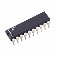
LTC1094ACN Linear Technology, LTC1094ACN Datasheet - Page 20

LTC1094ACN
Manufacturer Part Number
LTC1094ACN
Description
IC DATA ACQ SYS 10BIT 8CH 20-DIP
Manufacturer
Linear Technology
Type
Data Acquisition System (DAS), ADCr
Datasheet
1.LTC1091CN8PBF.pdf
(32 pages)
Specifications of LTC1094ACN
Resolution (bits)
10 b
Data Interface
Serial
Voltage Supply Source
Dual ±
Voltage - Supply
4.5 V ~ 10 V
Operating Temperature
-40°C ~ 85°C
Mounting Type
Through Hole
Package / Case
20-DIP (0.300", 7.62mm)
Lead Free Status / RoHS Status
Contains lead / RoHS non-compliant
Sampling Rate (per Second)
-
Available stocks
Company
Part Number
Manufacturer
Quantity
Price
Company:
Part Number:
LTC1094ACN
Manufacturer:
TI
Quantity:
7 818
Part Number:
LTC1094ACN
Manufacturer:
LT/凌特
Quantity:
20 000
Sharing the Serial Interface
The LTC1094 can share the same 2- or 3-wire serial
interface with other peripheral components or other
LTC1094s (see Figure 3). In this case, the CS signals
decide which LTC1094 is being addressed by the MPU.
ANALOG CONSIDERATIONS
1. Grounding
The LTC1091/LTC1092/LTC1093/LTC1094 should be used
with an analog ground plane and single point grounding
techniques.
The AGND pin (GND on the LTC1091/LTC1092) should be
tied directly to this ground plane.
The DGND pin of the LTC1093/LTC1094 can also be tied
directly to this ground plane because minimal digital noise
is generated within the chip itself.
The V
a 4.7 F tantalum with leads as short as possible. AV
DV
(LTC1093/LTC1094) should be bypassed with a 0.1 F
ceramic disk. For single supply applications, V
tied to the ground plane.
It is also recommended that the REF
be tied directly to the ground plane. All analog inputs
should be referenced directly to the single point ground.
Digital inputs and outputs should be shielded from and/or
routed away from the reference and analog circuitry.
A
20
LTC1091/LTC1092
LTC1093/LTC1094
PPLICATI
CC
CC
should be tied together on the LTC1094. The V
pin should be bypassed to the ground plane with
O
U
S
I FOR ATIO
U
Figure 3. Several LTC1094s Sharing One 3-Wire Serial Interface
OUTPUT PORT
2
SERIAL DATA
–
MPU
W
1
pin and the COM pin
0
3
3
U
8 CHANNELS
–
LTC1094
can be
CC
–
and
pin
CS
3
8 CHANNELS
LTC1094
Figure 4 shows an example of an ideal LTC1091 ground
plane design for a 2-sided board. Of course, this much
ground plane will not always be possible, but users should
strive to get as close to this ideal as possible.
2. Bypassing
For good performance, V
ripple. Any changes in the V
analog ground during a conversion cycle can induce
errors or noise in the output code. Because the V
pin of the LTC1091 defines the voltage span of the A/D
converter, its bypassing is especially important. V
and ripple can be kept below 1mV by bypassing the V
directly to the analog ground plane with a 4.7 F tantalum
with leads as short as possible. AV
tied together on the LTC1094. Figures 5 and 6 show the
effects of good and poor V
CS
Figure 4. Example Ground Plane for the LTC1091
3
8 CHANNELS
LTC1094
CS
3-WIRE SERIAL
INTERFACE TO OTHER
PERIPHERALS OR LTC1094s
1
2
3
4
TANTALUM
CC
4.7 F
CC
must be free of noise and
CC
bypassing.
8
7
6
5
V
voltage with respect to
CC
S
S
CC
LTC1091-4 F03
and DV
CC
should be
CC
CC
(V
CC
LTC1091-4 F04
noise
REF
pin
)


