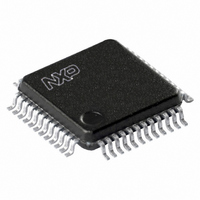
TDA8784HL/C4,151 NXP Semiconductors, TDA8784HL/C4,151 Datasheet - Page 10

TDA8784HL/C4,151
Manufacturer Part Number
TDA8784HL/C4,151
Description
IC ADC 10BIT 18MSPS 48-LQFP
Manufacturer
NXP Semiconductors
Type
ADCr
Datasheet
1.TDA8784HLC4518.pdf
(28 pages)
Specifications of TDA8784HL/C4,151
Package / Case
48-LQFP
Resolution (bits)
10 b
Sampling Rate (per Second)
18M
Data Interface
Serial
Voltage Supply Source
Analog and Digital
Voltage - Supply
4.75 V ~ 5.25 V
Operating Temperature
-20°C ~ 75°C
Mounting Type
Surface Mount
Product
Analog Front End
Interface Type
Serial (3-Wire)
Supply Voltage (max)
5.25 V
Supply Voltage (min)
2.5 V, 4.75 V
Supply Current
1 mA, 18 mA, 78 mA
Maximum Operating Temperature
+ 75 C
Minimum Operating Temperature
- 20 C
Mounting Style
SMD/SMT
Number Of Channels
1
Lead Free Status / RoHS Status
Lead free / RoHS Compliant
Other names
568-3607
935266802151
TDA8784HLBE-S
935266802151
TDA8784HLBE-S
Available stocks
Company
Part Number
Manufacturer
Quantity
Price
Company:
Part Number:
TDA8784HL/C4,151
Manufacturer:
NXP Semiconductors
Quantity:
10 000
Philips Semiconductors
2002 Oct 23
Clamps
g
g
Analog-to-Digital Converter (ADC)
f
t
t
SR
V
V
V
I
INL
DNL
t
Total chain characteristics (CDS + AGC + ADC)
t
N
V
V
Digital-to-analog converter (OFDOUT)
V
V
V
CLK(max)
CPH
CPL
ADCIN
d(s)
d
m(ADC)
m(CDS)
i(ADC)(p-p)
RB
RT
offset(fl-d)
n(i)(eq)(rms)
OFDOUT(p-p)
OFDOUT(0)
OFDOUT(255)
tot(rms)
18 Msps, 10-bit analog-to-digital
interface for CCD cameras
SYMBOL
CLK
ADC clamp transconductance
CDS clamp transconductance
maximum clock frequency
clock pulse width HIGH
clock pulse width LOW
clock input slew rate (rising
and falling edge)
ADC input voltage level
(peak-to-peak value)
ADC reference voltage output
code 0
ADC reference voltage output
code 1023
input current pin 10
integral non-linearity
differential non-linearity
sampling delay time
delay between SHD and CLK
total output noise (RMS value) f
maximum offset between CCD
floating level and CCD dark
pixel level
equivalent input noise voltage
(RMS value)
additional 8-bit control DAC
(OFD) output voltage
(peak-to-peak value)
DC output voltage for code 0
DC output voltage for
code 255
PARAMETER
at clamp level
at clamp level
10% to 90%
ramp input
ramp input
see Fig.5; 50% at rising
edges CLK and SHP:
transition full scale
code 0 to 1023;
f
f
V
f
AGC gain = 34.5 dB
AGC gain = 4.5 dB
cut(CDS)
cut(AGC)
cut(CDS)
cut(AGC)
i(CDS)
G
G
AGC
AGC
= 1200 mV
CONDITIONS
= 40 MHz;
= 120 MHz;
= 40 MHz;
= 40 MHz; note 2
= 4.5 dB
= 34.5 dB
10
18
15
15
0.5
2
200
MIN.
7
1.5
2
1.5
3.5
40
0.125
1.6
125
150
1.4
2.3
3.7
TYP.
0.6
0.2
Product specification
TDA8784
+120
5
+200
MAX.
1.5
0.75
mS
mS
MHz
ns
ns
V/ns
V
V
V
LSB
LSB
ns
ns
LSB
LSB
mV
V
V
V
UNIT
A
V
V


