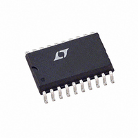
LTC1290CCSW#PBF Linear Technology, LTC1290CCSW#PBF Datasheet - Page 19

LTC1290CCSW#PBF
Manufacturer Part Number
LTC1290CCSW#PBF
Description
IC DATA ACQ SYS 12BIT 20-SOIC
Manufacturer
Linear Technology
Type
Data Acquisition System (DAS), ADCr
Datasheet
1.LTC1290CCSWPBF.pdf
(32 pages)
Specifications of LTC1290CCSW#PBF
Resolution (bits)
12 b
Sampling Rate (per Second)
50k
Data Interface
Serial, Parallel
Voltage Supply Source
Dual ±
Voltage - Supply
±5V
Operating Temperature
0°C ~ 70°C
Mounting Type
Surface Mount
Package / Case
20-SOIC (7.5mm Width)
Lead Free Status / RoHS Status
Lead free / RoHS Compliant
Available stocks
Company
Part Number
Manufacturer
Quantity
Price
A
Figure 6 shows an example of an ideal ground plane design
for a two-sided board. Of course, this much ground plane
will not always be possible, but users should strive to get
as close to this ideal as possible.
2. Bypassing
For good performance, V
ripple. Any changes in the V
analog ground during a conversion cycle can induce
errors or noise in the output code. V
be kept below 0.5mV by bypassing the V
the analog ground plane with a 22µF tantalum capacitor
and leads as short as possible. The lead from the device to
the V
V
that obtained from a voltage regulator (e.g., LT1761).
Figures 7 and 8 show the effects of good and poor V
bypassing.
3. Analog Inputs
Because of the capacitive redistribution A/D conversion
techniques used, the analog inputs of the LTC1290 have
capacitive switching input current spikes. These current
CC
PPLICATI
supply should have a low output impedance such as
CC
Figure 6. Example Ground Plane for the LTC1290
GROUND
ANALOG
supply should also be kept to a minimum and the
PLANE
O
TANTALUM
U
10
1
S
22µF
I FOR ATIO
CC
U
20
must be free of noise and
CC
voltage with respect to
V
CC
CC
W
noise and ripple can
CC
V
0.1µF
CERAMIC
DISK
pin directly to
–
U
LTC1290 F06
CC
spikes settle quickly and do not cause a problem. How-
ever, if large source resistances are used or if slow settling
op amps drive the inputs, care must be taken to insure that
the transients caused by the current spikes settle com-
pletely before the conversion begins.
Source Resistance
The analog inputs of the LTC1290 look like a 100pF
capacitor (C
shown in Figure 9. C
“+” and “–” inputs once during each conversion cycle. Large
external source resistors and capacitances will slow the
settling of the inputs. It is important that the overall RC time
constants be short enough to allow the analog inputs to
completely settle within the allowed time.
Figure 7. Poor V
Noise and Ripple Can Cause A/D Errors
Figure 8. Good V
Noise and Ripple on V
IN
) in series with a 500Ω resistor (R
IN
HORIZONTAL: 10µs/DIV
HORIZONTAL: 10µs/DIV
gets switched between the selected
CC
CC
Bypassing.
Bypassing Keeps
CC
Below 1mV
LTC1290
19
CS
V
ON
CC
1290fe
) as


